The electrical circuit of the oscilloscope c1 68.
Attention!!! Delivery of ALL devices that are listed on the site takes place throughout the territory of the following countries: Russian Federation, Ukraine, Republic of Belarus, Republic of Kazakhstan and other CIS countries.
In Russia, there is an established delivery system to such cities: Moscow, St. Petersburg, Surgut, Nizhnevartovsk, Omsk, Perm, Ufa, Norilsk, Chelyabinsk, Novokuznetsk, Cherepovets, Almetyevsk, Volgograd, Lipetsk Magnitogorsk, Tolyatti, Kogalym, Kstovo, Novy Urengoy, Nizhnekamsk, Nefteyugansk, Nizhny Tagil, Khanty-Mansiy sk, Yekaterinburg, Samara, Kaliningrad, Nadym, Noyabrsk, Vyksa, Nizhny Novgorod, Kaluga, Novosibirsk, Rostov-on-Don, Verkhnyaya Pyshma, Krasnoyarsk, Kazan, Naberezhnye Chelny, Murmansk, Vsevolozhsk, Yaroslavl, Kemerovo, Ryazan, Saratov, Tula, Usinsk, Orenburg, Novotroitsk, Krasnodar, Ulyanovsk, Izhevsk, Irkut sk, Tyumen, Voronezh, Cheboksary, Neftekamsk, Veliky Novgorod, Tver, Astrakhan, Novomoskovsk, Tomsk, Prokopyevsk, Penza, Uray, Pervouralsk, Belgorod, Kursk, Taganrog, Vladimir, Neftegorsk, Kirov, Bryansk, Smolensk, Saransk, Ulan-Ude, Vladivostok, Vorkuta, Podolsk, Krasnogorsk, Novouralsk, Novorossiysk , Khabarovsk, Zheleznogorsk, Kostroma, Zelenogorsk, Tambov, Stavropol, Svetogorsk, Zhigulevsk, Arkhangelsk and other cities of the Russian Federation.
In Ukraine, there is an established delivery system to such cities: Kiev, Kharkov, Dnipro (Dnepropetrovsk), Odessa, Donetsk, Lvov, Zaporozhye, Nikolaev, Lugansk, Vinnitsa, Simferopol, Kherson, Poltava, Chernihiv, Cherkasy, Sumy, Zhytomyr, Kirovograd, Khmelnitsky, Rivne, Chernivtsi, Ternopil, Ivano-Frankivsk, Lutsk, Uzhgorod and other cities of Ukraine.
In Belarus, there is an established delivery system to such cities: Minsk, Vitebsk, Mogilev, Gomel, Mozyr, Brest, Lida, Pinsk, Orsha, Polotsk, Grodno, Zhodino, Molodechno and other cities of the Republic of Belarus.
In Kazakhstan, there is an established delivery system to such cities: Astana, Almaty, Ekibastuz, Pavlodar, Aktobe, Karaganda, Uralsk, Aktau, Atyrau, Arkalyk, Balkhash, Zhezkazgan, Kokshetau, Kostanay, Taraz, Shymkent, Kyzylorda, Lisakovsk, Shakhtinsk, Petropavlovsk, Rider, Rudny, Semey, Taldykorgan, Temir tau, Ust-Kamenogorsk and other cities of the Republic of Kazakhstan.
Manufacturer TM "Infrakar" is a manufacturer of multifunctional devices such as a gas analyzer and smoke meter.
If the website does not contain the information you need about the device in the technical description, you can always contact us for help. Our qualified managers will clarify for you the technical characteristics of the device from its technical documentation: operating instructions, passport, form, operating manual, diagrams. If necessary, we will take photos of the device, stand or device you are interested in.
You can leave feedback on the device, meter, device, indicator or product purchased from us. Your review, with your consent, will be published on the site without specifying contact information.
The description for the devices is taken from the technical documentation or from the technical literature. Most of the product photos are taken directly by our specialists before the goods are shipped. The description of the device provides the main technical characteristics of the devices: nominal value, measurement range, accuracy class, scale, supply voltage, dimensions (size), weight. If on the site you saw a discrepancy between the name of the device (model) technical specifications, photo or attached documents - let us know about it - You will receive a useful gift along with the purchased device.
If necessary, you can specify the total weight and dimensions or the size of a separate part of the meter in our service center. If necessary, our engineers will help you choose a complete analogue or the most suitable replacement for the device you are interested in. All analogues and replacements will be tested in one of our laboratories for full compliance with your requirements.
Our company carries out repair and maintenance of measuring equipment for more than 75 different manufacturing plants of the former USSR and the CIS. We also carry out such metrological procedures: calibration, taring, graduation, testing of measuring equipment.
Devices are delivered to the following countries: Azerbaijan (Baku), Armenia (Yerevan), Kyrgyzstan (Bishkek), Moldova (Kishinev), Tajikistan (Dushanbe), Turkmenistan (Ashgabat), Uzbekistan (Tashkent), Lithuania (Vilnius), Latvia (Riga), Estonia (Tallinn), Georgia (Tbilisi).
Zapadpribor LLC is a huge selection of measuring equipment at the best price-quality ratio. So that you can buy devices inexpensively, we monitor competitors' prices and are always ready to offer more low price. We only sell quality products at the best prices. On our website you can buy cheap both the latest innovations and time-tested devices from the best manufacturers.
The site constantly operates the promotion "Buy for best price» - if on another Internet resource the product presented on our website has a lower price, then we will sell it to you even cheaper! Buyers also receive an additional discount for leaving a review or photos of the use of our products.
The price list does not contain all the range of products offered. Prices for goods not included in the price list can be found by contacting managers. You can also get from our managers detailed information about how to buy cheap and profitable measuring instruments Wholesale and Retail. phone and Email for advice on the purchase, delivery or receiving a discount are given above the product description. We have the most qualified employees, high-quality equipment and a favorable price.
Zapadpribor LLC is an official dealer of measuring equipment manufacturers. Our goal is to sell goods High Quality with the best price offers and service for our clients. Our company can not only sell the device you need, but also offer Additional services for its verification, repair and installation. So that you have a pleasant experience after buying on our website, we have provided special guaranteed gifts for the most popular products.
The META plant is a manufacturer of the most reliable technical inspection devices. The STM brake tester is produced at this plant.
If you can repair the device yourself, then our engineers can provide you with a complete set of necessary technical documentation: circuit diagram, TO, RE, FO, PS. We also have an extensive database of technical and metrological documents: specifications(TU), terms of reference (TOR), GOST, industry standard (OST), verification methodology, certification methodology, verification scheme for more than 3500 types of measuring equipment from the manufacturer this equipment. From the site you can download all necessary software(program, driver) necessary for the operation of the purchased device.
We also have a library of legal documents that are related to our field of activity: law, code, resolution, decree, temporary situation.
At the request of the customer, verification or metrological certification is provided for each measuring device. Our employees can represent your interests in such metrological organizations as Rostest (Rosstandart), Gosstandart, Gospotrebstandart, TsLIT, OGMetr.
Sometimes customers may enter the name of our company incorrectly - for example, zapadpribor, zapadprylad, zapadpribor, zapadprilad, zakhіdpribor, zakhіdpribor, zahidpribor, zahidprilad, zahidprіbor, zahidprybor, zahidprylad. That's right - zapadpribor.
Zapadpribor LLC is a supplier of ammeters, voltmeters, wattmeters, frequency meters, phase meters, shunts and other devices from such measuring equipment manufacturers as: PO Elektrotochpribor (M2044, M2051), Omsk; JSC Instrument-Making Plant Vibrator (M1611, Ts1611), St. Petersburg; Krasnodar ZIP OJSC (E365, E377, E378), ZIP-Partner LLC (Ts301, Ts302, Ts300) and ZIP Yurimov LLC (M381, Ts33), Krasnodar; OJSC "VZEP" ("Vitebsk plant of electrical measuring instruments") (E8030, E8021), Vitebsk; JSC Elektropribor (M42300, M42301, M42303, M42304, M42305, M42306), Cheboksary; JSC "Elektroizmeritel" (Ts4342, Ts4352, Ts4353) Zhytomyr; PJSC "Uman Plant" Megommetr "(F4102, F4103, F4104, M4100), Uman.
Somehow I set out to purchase an oscilloscope for amateur purposes. There wasn’t enough money for a good digital one, and he didn’t really need any bells and whistles. Therefore, it was decided to start to purchase an analog one, from the time of the Soviets. Found an advertisement and went to buy. The owner assured that he was in working order. An on-site test in his garage showed that the appliance was not working. It turned out he did not turn on for about two years. Of the visible, only the backlight of the scale worked. As a result, the owner dropped the price, and I took the device at a cheap price. Previously, I had not repaired oscilloscopes, but there was a hope that all repairs would be reduced to replacing electrolytes, since, according to the owner, the device was working before it lay in the garage.
Arriving home and plugging the device into a power outlet, a strong heating of the power transistors on the rear panel was discovered. I decided to first disassemble and replace all the electrolytes. Which he did.
Just in case, I changed transistors 1-T1, 1-T2, 1-T3, T4, T5. In the process, I also found a charred 1-R28 and the Brightness control. I cleaned all the contacts with a special spray and alcohol. After all manipulations osc. turned on, there is a reaction to touching the probe with a finger. Brightness, vertical position is not adjustable. Astigmatism and focus adjust, but I can’t set a beautiful point, the cross turns out and is 1 cell below the center. When a signal is applied from the calibrator to the input, it shows garbage.
The main voltages were measured on the test block. All were underestimated. The stabilizer works, keeps its 8V and is regulated by a trimmer. I tried to turn it on without load by disconnecting the 1-Sh3 block and removing the block from the tube. Voltage is also low. There is a beam in the center, but the brightness is not adjustable. I measured the frequency on the collectors 1-T1, 1-T2 with a multimeter - about 1.7 kHz (according to the book it should be 2 kHz + -300 Hz). When working with connected and disconnected pads, transistors 1-T1, 1-T2 and res. 1R-27 get very hot.
 |
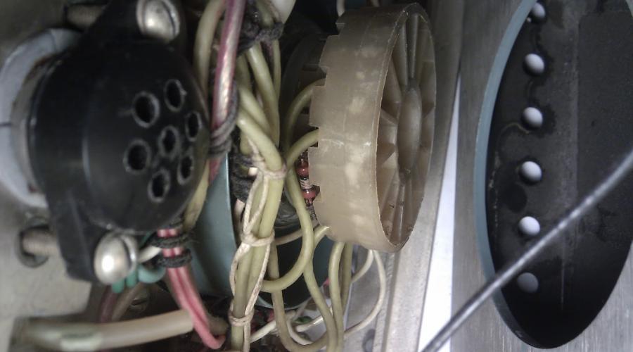
| Burnt resistor 1R-27 and a hot transistor. |
Then soldered the resistor 1R-27. Enabled. The beam lit up brighter than before and ran across the screen Reacted to the handles (except for brightness). After a minute, everything went dark. The voltages on 1-Sh3 have dropped to 1-10V and are jumping. On the stabilizer, it also fell somewhere to 4-6V. Measured and with the CRT panel removed and dressed.
Subsequent manipulations revealed that the D2 diode on the 80V power supply burned out again. Restored. Turned on with the CRT panel removed and soldered 1R-27. Everything else is connected. All voltages on 1-Sh3 are normal. The transistors are warm, as they should be. I solder 1R-27 on the removed CRT panel, the voltages sag almost 2 times. When I turn it on with a CRT panel on with a soldered 1R-27, crackling is heard in the tube, and then diode D2 flies out again.
From everything, it became clear that the filament winding of the 1-Tr1 transformer was shorting to some of the secondary circuits. It was decided to power the glow separately by unsoldering the wires from 1-Tr1 and applying 6.3V to them from a separate transformer. When applying separate power to the glow, the oscilloscope worked as expected. Brightness control appeared after replacing the capacitor 1-C13. It also turned out to be broken. The transformer was built into the case of the oscilloscope, which now serves me safely in my home laboratory.
\S1 Oscilloscopes \S1-68 Universal Oscilloscope
Analog oscilloscope C1-68
Price at the time of adding to the catalog (October 2016): 24,500.00 rubles.
PURPOSE OF THE UNIVERSAL OSCILLOSCOPE С1-68
Oscilloscope C1-68 designed for research electrical signals in the bandwidth of 0 - 10 MHz by visual observation on the screen of a cathode ray tube (CRT), measuring their amplitude and time parameters on the screen scale. It can be used for repair, maintenance and troubleshooting of electronic equipment, including hard-to-reach objects. device C1-68 characterized by ease of operation and maintenance, structural strength, high temporal and temperature stability, low weight and overall dimensions. This model of a portable oscilloscope has found its wide application not only among radio amateurs, but also among professionals.
MAIN TECHNICAL CHARACTERISTICS OF THE C1-68 OSCILLOSCOPE
- Number of beams (channels) CRT: single beam
- Measured voltage range: 2 mV - 200 V
- Range of measured time intervals: 2 µs – 16 s
- Bandwidth: 0 - 1 MHz
- Rise Time: 350 ns
- Signal amplitude measurement error: no more than 5%
- Time interval measurement error: no more than 5%
- Emission to PH: no more than 10%
- Beam Line Width: 0.7mm
- Horizontal screen area: 80 mm
- Vertical screen area: 60 mm
- Power supply: 220 V, 50 Hz; 115 V, 400 Hz
- Power consumption: 40 V*A
- Operating temperature range: -10... +50 °C
- Y Channel Settings
- Channel Sensitivity: 1 mV/div - 5 V/div
- Channel input impedance: 1 MΩ
- Channel input capacitance: 50 pF
- Channel X Settings
- Minimum sweep duration: 2 µs/div
- Sweep duration maximum: 2 sec/div
- External clock amplitude: 0.5 - 50 V
- External sync frequency range: 1 Hz - 1 MHz
- External sync input impedance: 50 kOhm
- Channel Z Settings
- Channel frequency range: 20 Hz - 0.2 MHz
- Input voltage range: 20 - 50 V
- Channel input impedance: 10 kOhm
- Calibration Channel Parameters
- Calibration signal frequency: square wave 2 kHz
- Calibration signal voltage: 0.1 or 1 V
- Weight: 10 kg
- Dimensions: 274x206x440 mm
Variants of spelling: C1-68, C1-68
The present technical description and operating instructions are intended to familiarize persons operating the device with the device and the principle of operation, the basic rules for operation, maintenance, simple repair and transportation of the device.
Oscilloscope C1-68 is complex electronic device, providing a relatively high measurement accuracy and ease of use. Thanks to the application semiconductor devices The oscilloscope is small in size and has low power consumption.
Trouble-free operation of the device is ensured by regular maintenance. Types and frequency of work on. , maintenance are set out in Section 11. The oscilloscope was tuned and adjusted using a variety of precision instruments, therefore, any overshoots inside the device should be avoided.
Repair of the device should be carried out by persons with special training, familiar with the device and the principles of operation of this device, in the conditions of specially equipped workshops. The device contains life-threatening voltages, therefore, before opening and repairing the device, be sure to read the safety instructions in section 6.
To exclude the possibility of mechanical damage to the device, violation of the integrity of the coatings, you must follow the rules for storing and transporting the device, set out in sections 12 and 13.
When operating the instrument in a tropical climate, it is recommended to operate it in an air-conditioned room.
In a humid tropical climate, when operating the device in room conditions without air conditioning, it is necessary to first turn on the device for at least two hours in order to warm it up.
Purpose
Universal oscilloscope S1-68 is designed to observe and study the form of electrical processes by visual observation and measurement of their time and amplitude values. According to the accuracy of signal reproduction, measurement of time and amplitude values, the device belongs to II-III classes of GOST 9810-69.
Terms of Use:
working ambient temperature from minus 10
limiting temperature from minus 50 to +60°С; relative air humidity up to 95% at temperature
The device works normally after exposure (in the stowage box) to shock loads:
multiple action with acceleration up to 15g pulse duration then 5 to 10 µs;.
single action with acceleration up to 75g pulse duration from 1 to 10 µs.
The device is resistant to cyclic changes in the temperature of the surrounding air from the limiting positive to the limiting negative.
The device is available in two versions;
desktop I22.044.053 rack I22.044.054.
Technical data
Oscilloscope C1-68 provides:
a) observation of the shape of pulses of both polarities with a duration of 2 μs to 16 e with a swing of 1 mV to 300 V;
b) observation of periodic signals in the frequency range from 0.06 Hz to 1 MHz;
c) measurement of the amplitudes of the studied signals with a swing from 2 mV to 300 V, and with an external divider 1:10 - from 20 mV to 350 V;
d) measurement of time intervals - from 2 μs to 16 s.
3. 2. The working part of the screen: is 60 mm vertically and 80 mm horizontally.
3. 3. The thickness of the beam line does not exceed 0.7 mm, and with a sensitivity of 10 mm / mV (1 mV / cm) - 1 mm.
3. 4. The vertical beam deflection path amplifier has the following parameters:
a) bandwidth from 0 to 1 MHz with uneven amplitude-frequency response in the band no more than 3 dB,
and in the frequency range from 0 to 200 kHz - no more than ± 4%;
b) the rise time of the transient response of the path does not exceed 0.35 µs, and the settling time is 1.1 µs.
The settling time is the time interval from the level of 0.1 amplitude until the moment when the value of the transient response after the release reaches a predetermined value of the steady state ripple;
c) the nonlinearity of the amplitude characteristic in the working part of the screen does not exceed 5%;
d) the magnitude of the surge on the transient characteristic does not exceed 10% with a rising front of 0.11 μs;
e) input impedance of the device at open entrance- 1 MΩ ± 2% with an input capacitance of 50 pF ± 10% - With a remote divider 1:10, the input impedance of the amplifier is 10 MΩ ± ± 10%, and the input capacitance does not exceed 15 pF. The error of division of the remote divider does not exceed ±10%;
The input of the device can be open or closed, the input of the remote divider 1:10 is open.
f) the total DC and AC allowable voltage of the signal applied to the closed input of the device must not exceed 350 V.
Drift of the zero line on the oscilloscope screen after 15 min. warm-up does not exceed 3 mV (30 mm) for 30 minutes of operation.
The short-term drift of the zero line does not exceed 0.3 mV (3 mm) for 1 min.
The drift of the zero line when the supply voltage changes by ± 10% does not exceed 0.3 mV.
The drop in the peak of the steady value of the transient characteristic for a duration of 10 μs with a closed input of the device does not exceed 10%.
The maximum calibrated sensitivity of the vertical deflection path is 10 mm/mV.
Deviation coefficients (switch positions V/cm, mV/cm) are set: a) stepwise from 1 mV/cm to 5 V/cm with an overlap of 2 and 2.5 times and the possibility of multiplication (decrease in sensitivity) by 10;
b) smoothly with an overlap of at least 2.5 times.
The error of the calibrated deviation coefficients does not exceed ±4%, and the error of the coefficient of 1 mV / cm - ±7% under normal conditions and, respectively, ±8% and ±10% - in operating conditions with a simultaneous change in mains voltage by ±10%.
The main error in measuring the amplitudes of rectangular pulse signals with a duration of 2 μs, a repetition rate of up to 10 kHz and an image size of 2 to 6 divisions should not exceed ± 5% - with a calibrated sensitivity from 5 mm / mV (2 mV / cm) to 0.2 mm / V (50 V / cm); ±8% - at a calibrated sensitivity of 10 mm/mV (1 mV/cm) multiplied by 1 or 10.
The error in measuring the amplitudes of pulse signals under operating conditions with a simultaneous change in the supply voltage does not exceed ±10%, and with a calibrated sensitivity of 10 mm/mV (1 mV/cm) - ±12%.
The error in measuring the amplitudes of sinusoidal signals under operating conditions in the frequency range from 0 to 200 kHz does not exceed ±10%, and with a sensitivity of 10 mm/mV (1 mV/cm) multiplied by 1 or 10 - ±12%.
3. 9. The internal calibration voltage source generates U-shaped pulses with a frequency of 2 kHz, an amplitude of 100 mV and 1 V with an amplitude and frequency error of no more than ± 1.5% under normal conditions and no more than ± 2.5% - in operating conditions with a simultaneous change in mains voltage by ± 10%.
The pulse asymmetry does not exceed 20%. „ 3. 10. The sweep generator can operate in a periodic; or standby mode and has the following options:
a) the range of calibrated sweep durations (calibrated sweep coefficients) from 2 s/cm to 2 μs/cm is divided into 19 fixed subranges (sweep coefficients) with an overlap of 2 and 2.5 times and the possibility of a five-fold extension of the sweep (five-fold reduction of the sweep coefficients in the X0.2 position).
Smooth overlapping of each subband at least 2.5 times.
b) the error of the calibrated sweep coefficients does not exceed ±4%, and when using the sweep multiplier - ±7% under normal conditions and, respectively, ±8% and ±10% - under operating conditions with a simultaneous change in the mains voltage by ±10%;
c) the non-linearity of the sweeping voltage of the working part of the sweep (5 mm each at the beginning and end of the sweep line - without stretching and 10 mm each - when using (sweep stretching) does not exceed 5%, and with a fivefold stretching (X 0.2) -10%.
The main error in measuring time intervals with a measured horizontal image size of 3 to 8 divisions does not exceed ±5% without stretching and ±8% with stretching.
The measurement error of time intervals under operating conditions does not exceed ±10% - without stretching and ±12% - with stretching.
The internal synchronization of the sweep is carried out by the signal under study of any polarity with a minimum image size of 3 mm in the frequency range from 1 Hz to 1 MHz and pulse signals with a duration of 2 μs or more.
External synchronization is provided with the amplitude of the synchronizing signal from 0.5 V to 50 V in the frequency range from 1 Hz to 1 MHz, and pulse signals with a duration of 2 μs.
The input impedance of the external synchronization input is not less than 50 kOhm in the position of the synchronization switch 1:1> and not less than 500 kOhm - in the position 1:10 with an input capacitance of 50 pF.
The minimum sweep repetition rate at which the observation of the signal under study is ensured at the fastest sweep does not exceed 250 Hz.
The delay of the start of the sweep relative to the synchronization signal does not exceed 0.3 μs.
The device has the ability to supply the investigated voltages in the frequency band from 20 Hz to 10 MHz directly to the deflecting plates of the cathode ray tube (CRT) through external transition capacitors with a capacity of 0.1 μF and U work equal to 400 V. The input to the plates is symmetrical, open.
The input resistance is 1 MΩ ± 20% with an input capacitance of not more than 20 pF.
Input Sensitivity PLATE Y - 1.0 mm/V, PLATE X - 0.6 mm/V.
3. 16. The device provides for the possibility of deflecting the beam horizontally by external voltage.
The horizontal beam deflection channel amplifier has the following parameters:
a) the unevenness of the amplitude-frequency characteristic does not exceed 3 dB in the frequency range from 0 to 500 kHz;
b) sensitivity not less than 1 cm/V.
c) input resistance not less than 50 kOhm with input capacitance not more than 30 pF;
X - open cm / V.
must be from 20V to 50V in the frequency range from 20Hz to 200kHz.
The input impedance of the input Z is 1 MΩ ± 20% with an input capacitance of not more than 35 pF.
The value of low-frequency noise at a sensitivity of 10 mm / mV (1 mV / cm) does not exceed 100 μV (1 mm) with an input jack protected from external interference.
The device provides a sawtooth voltage output from a sweep generator with an amplitude ranging from 5 to 12V at a load of at least 20 kOhm with a parallel capacitance of not more than 100 pF.
The device is powered by:
from the network alternating current voltage 220 V ± 10%, frequency 50 Hz ± 1% and 60 Hz ± 1% and harmonic content up to 5%;
and harmonic content up to 5%;
from source direct current voltage 12.6V ± 10%, and through an adapter block with damping resistance - from a DC source with a voltage of 24 V ± 10%.
The maximum power consumed from the network does not exceed 40VA,
The current consumed by the device when powered by a 12.6V DC source does not exceed 1.8 A.
The warm-up time of the device does not exceed 15 minutes.
The time of continuous operation of the device should not exceed 16 hours.
Note. The device allows a slight change in sensitivity and a beam shift parallel to the scale lines up to 2 mm when the beam brightness changes to the maximum.
The mass of the device does not exceed: for desktop - 10 kg; for rack - 14 kg. The weight in a transport container does not exceed: for desktop execution - 45 kg; for rack-mount design - 46 kg.
Overall dimensions of the device: desktop execution - 274X182X440 mm; rack-mount - 520X160X510 mm; Overall dimensions of the device in the package:
for desktop version - 410X276X483 mm (in a box); 288X204X453 mm (card, box);
for rack version - 533X181X533 mm.
Overall dimensions of a transport container:
for desktop execution - 533X407X682 mm (with stacking box);
414X341X723 mm (with cards, box);
for rack version - 656X341X851 mm.


Notes:
1. S1-68 rack-mount oscilloscope I22.044.054 is supplied by special order in accordance with the supply contract. For devices with QCD acceptance, delivery in a polystyrene foam box instead of a cardboard one is possible.
2. Adapter block I23.656.020 is used when powered by a 24 BN DC voltage source and is supplied by special order in accordance with the supply agreement.
3. The time counter ESV-2.5-12.6/0 is installed in the device upon special request in accordance with the supply contract.
OSCILLOSCOPE UNIVERSAL i 1977 OSCILLOSCOPE UNIVERSAL С1-68 TECHNICAL DESCRIPTION AND OPERATING INSTRUCTIONS Album 1977 № 1 ATTENTION! 1. Before turning on the device in the power supply, check the correct installation of the toggle switch "220V50Hz-115V400HZ" on the rear E "i.^aOopa l type of connected power cord. 2. When using an external divider 1: 10 for measurements, the guaranteed measurement accuracy can be ensured if the vertical amplifier is calibrated with an external divider. The divider must be compensated. 3. In order to reduce the effort, switching the sweep switch "DURATION" should be done with light pressure of the handle along the longitudinal axis of the switch f CONTENTS 1. 2. 3. 4. 5. INTRODUCTION FUNCTION TECHNICAL DATA COMPOSITION OF THE PRODUCT . 6. SAFETY PRECAUTIONS 7. PREPARATIONS FOR OPERATION 7.1 General provisions 7. 2. Preparation for measurements 8. ORDER OF WORK . . . 8. 1. Waiting sweep with synchronization by the signal under study 8. 2. Continuous sweep with synchronization by the signal under study 8. 3. Synchron Ization from an external source 8. 4. Sweep from an external source. . 8. 5. External modulation of the beam in terms of brightness. 8. 6 Supply of the studied voltages directly to the CRT plates. 8. 7. Measurement of time intervals 8. 8. Measurement of frequency. . . . 8. 9. Measurement of the amplitude of the investigated spgn. 9. VERIFICATION OF O S C I L L O G R A F A. 9. I. Operations and means of verification. 9. 2. Verification conditions and preparation for it 9. 3. Verification. . . . 9. 4. Formulation of verification results 10. CHARACTERISTIC MALFUNCTIONS II METHODS FOR THEIR ELIMINATION Yu. I. General instructions Yu. 11. MAINTENANCE P. I General instructions 11.2. visual inspection. Page 7 8 8 13 14 14 16 36 40 40 40 . 4 1 46 46 46 47 . 4 7 47 . 4 7 48 49 50 51 51 54 5 4 60 6 61 61 62 65 67 67 7 flax meposreistbemim in the 6 case of the instrument pontoon chST-stoics 5. OMLT reistors according to GOST EL 7NZ "7 | L. Pesucmopw SMPpo 0 * 0467 056Tb Universal oscilloscope I Capacitors kppo DXC 160 043TU 8 ConEensagoors KT go GOST 7159-H "68 S Numbers O tss.ybno with * epy apektricesksh arrischilia * “Tramietors T2T3 Ilote U2) are selected in accordance with appendix 7 and? 2 044 0S3TQ No. QV4 0S53S AisPTs 1-(kS "/l" Ots logger universal a-68 Electrical circuit diagram g ^ I I. 3. Internal and external cleaning 67 11. 4. Lubrication of the device. . . 68 11. 5. Adjustment of the ELT circuit 68 11. 6. Adjustment 68 11. 7. Adjustment and calibration of the sweep generator duration 69 I I. 8. Adjustment of the ELT beam control circuit .. 70 11.9. Adjustment of the horizontal beam deflection amplifier 70 11. 10. Adjustment of the calibrator . . . . 7 1 II. I. Adjustment of the input atten 71 P. 12. Adjusting the vertical deflection amplifier 72 11. 13. Adjusting the power unit . 7 3 12. STORAGE REGULATIONS 75 13. TRANSPORTATION 75 APPENDICES . . . 77 instrument resistance 85 3. Map impulse voltage. . . 91 4. Drawings of the location of the main elements. . . 107 5. Winding data of transformers 114 6. Scheme of the transition chain for determining input parameters 116 7. Selection technique field effect transistors i 17 8. Adapter block I23.656.020. . . . 117 9. Electrical circuit diagram of the divider I: 10 117 10. List of accepted abbreviations and symbols. 118 11. Electrical circuit diagram I22.044.053EZ. List of elements 119 ^ L "External external device 1. INTRODUCTION This technical description and operating instructions are intended to familiarize persons operating the device with the device and the principle of operation, basic rules and operation, maintenance, simple repair and transportation of the device. S1-68 oscilloscope is a complex electronic device that provides a relatively high accuracy of "Measurements and ease of use. Due to the use of semiconductor devices, the oscilloscope has small dimensions and low power consumption. Trouble-free operation of the device is ensured by regular maintenance. The types and frequency of maintenance work are described in Section 11. The oscilloscope was set up and adjusted using a variety of precision instruments, so any overshoots inside the device should be avoided. be sure to familiarize yourself with the safety instructions set out in section 6. To exclude the possibility of mechanical damage to the device, violation of the integrity of the coatings, you must follow the rules for storing and transporting the device, set out in sections 12 and 13. When using the device® in tropical climate conditions, it is recommended to operate it in an air-conditioned room. 7 In a humid tropical climate, when operating the instrument in room conditions without air conditioning, the instrument must first be turned on for at least two hours to warm up. 2. PURPOSE S1-68 universal oscilloscope is designed to observe and study the form of electrical processes by visual.observation.and measurement of their time and amplitude values. About the accuracy of signal reproduction, measurement of time and amplitude values, the device belongs to I I - I I I classes of GOST 9810-69. Operating conditions: operating temperature of the ambient air from minus 10 to + 50 ° С; limiting temperature from minus 50 to +60 o C; relative air humidity up to 95% at temperatures up to +30°С. The device normally works after exposure (in the stacking box) to shock loads: multiple action with acceleration up to 15g with a pulse duration from 5 to 10 ms; single action with acceleration up to 75g pulse duration from 1 to 10 ms. The device is resistant to cyclic changes in ambient temperature from the limiting positive to the limiting negative. The device is produced in two versions: desktop I22.044.053; rack I22.044.054. 3. TECHNICAL DATA 3. 1. The S1-68 oscilloscope provides: a) observation of the shape of pulses of both polarities with a duration of 2 μs to 16 s with a span of 1 mV to 300 V; b) observation of periodic signals in the frequency range from 0.06 Hz to I MHz; c) measurement of the amplitudes of the studied signals with a swing from 2 mV to 300 V, and with an external divider 1:10 - from 20 mV to 350 V; d) measurement of time intervals - from 2 microseconds to No. sec. 3. 2. The working part of the screen is 60 mm vertically and 80 mm horizontally. 10 3. 3. The thickness of the beam line does not exceed 0.7 us, and with a sensitivity of 10 mm / mV (1 mV / cm) - 1 mm. 3. 4. The amplifier of the vertical deflection path of the beam has the following parameters: a) a bandwidth of 0 to 1 MHz with an uneven frequency response in the band no more than 3 dB, and in the frequency range from 0 to 200 kHz - no more than ± 4%; b) the rise time of the transient response of the path does not exceed 0.35 µs, and the settling time is 1.1 µs. The settling time is the time interval from the level of 0.1 amplitude to the moment when the value of the transient response after the surge reaches the specified value of the steady-state value non-uniformity: c) the non-linearity of the amplitude response in the working part of the screen does not exceed 5%; d) the magnitude of the surge - on the transient characteristic does not exceed 10% with a rise front of 0.11 μs; e) the input resistance of the device with an open input - 1 M ohm ± 2% with an input capacitance of 50 pF ± 10%. With a remote divider 1: 1 0 the input impedance of the amplifier is 10 M ohm ± ± 1 0%, and the input capacitance does not exceed 15 pF. The error of division of the remote divider does not exceed ± 10%; The input of the device can be open or closed, the input of the remote divider 1:10 is open. f) the total DC and AC allowable voltage of the signal applied to the closed input of the device must not exceed 350 volts. 3. 5. Oscilloscope base line drift after 15 minutes of warm-up does not exceed 3 mV (30 mm) in 30 minutes of operation. The short-term drift of the zero line does not "exceed 0.3 mV (3 mm) per 1 minute. The drift of the zero line with a change in the supply voltage by ± 10% does not exceed 0.3 mV. 3. 6. Siats peaks of the steady value of the transient response with a duration of 10 ms with a closed input of the device does not exceed 10%. 3. 7. The maximum calibrated sensitivity of the vertical deflection path is 10 mm/mV Deviation coefficients (switch positions "V/cm, mV/cm") are set: a) stepwise from 1 mV/cm TO 5 v/cm with overlapping by 2 and 2.5 times and the possibility of multiplication (decrease in sensitivity) by 10; b) smoothly with overlapping at least 2.5 times. 7% in (normal conditions and, respectively, ± 8% and ± 10% - in operating conditions with a simultaneous change in mains voltage by ± 10%. 3. 8. The main error in measuring the amplitudes of rectangular pulse signals with a duration of 2 μs, a repetition rate of up to 10 kHz and an image size from 2 to 6 divisions should not exceed ± 5% - with a sensitivity adjustment of 5 mm / ml (2 mv/cm) up to 0.2 mm/v (50 v/ohm); ± 8% - with a calibrated sensitivity of 10 mm / mV (1 mV / cm), multiplied by 1 or 10. The error in measuring the amplitudes of pulse signals under operating conditions with a simultaneous change in the supply voltage does not exceed ± 10%, and three calibrated sensitivity of 10 mm / mV (1 mV / cm) - ± 12%. The error in measuring the amplitudes of sinusoidal signals under operating conditions in the frequency range from 0 to 200 kHz does not exceed ± 10%, and with a sensitivity of 10 mm / mV (1 mV / cm), narrowed by 1 or 10, - ± 12%. 3. 9. The internal calibration voltage source generates U-shaped pulses with a frequency of 2 kHz, an amplitude of 100 mV and 1 V with an amplitude and frequency error of no more than ± 1.5% under normal conditions and no more than ± 2.5% - in operating conditions with a simultaneous change in mains voltage by ± 10%. The pulse asymmetry does not exceed 20%. 3. 10. The sweep generator can operate in a periodic or standby mode and has the following parameters: a) The range of calibrated sweep durations (calibrated sweep coefficients) from 2 sec/cm to 2 μs/cm is divided into 19 fixed subranges (sweep coefficients) with an overlap of 2 and 2.5 times and the possibility of a five-fold extension of the sweep (five-fold reduction sweep coefficients in the “x0.2” position). Smooth overlapping of each subrange. not less than 2.5 times. b) the error of the calibrated sweep coefficients does not exceed ± 4%, and when using the sweep multiplier - ± 7% under normal conditions and, respectively, ± 8% and ± 10% - E operating conditions with a simultaneous change in the supply voltage by ± 10%". 10 3. P. The main measurement error of time intervals with a measured horizontal image size of 3 to 8 divisions does not exceed ± 5% without stretching and ± 8% - with stretching. The error of measuring time intervals under operating conditions does not exceed ± 10% - without stretching and ± 12% - with stretching 3. 12. Internal synchronization of the sweep is carried out by the signal under study of any polarity with a minimum image size of 3 mm in the frequency range from 1 Hz to 1 MHz and pulse signals with a duration of 2 μs or more. External synchronization is provided with the amplitude of the synchronizing signal from 0.5 to 50 V in the frequency range from 1 Hz to 1 MHz, and pulse signals with a duration of 2 μs. The input resistance of the external synchronization input is not less than 50 kΩ in the “1:1” position of the synchronization switch and not less than 500 kΩ in the “1: 1 0” position with an input capacitance of 50 pF. The entrance "-£) -" is open. 3. 13. The minimum sweep repetition rate at which the observation of the signal under study is ensured at the fastest sweep does not exceed 250 Hz. 3. 14. The delay. of the beginning of the sweep relative to the synchronization signal does not exceed 0.3 μs. 3. 15. The device has the ability to supply the voltages under study in the frequency band from 20 Hz to 10 MHz directly to the deflecting plates of the cathode ray tube (E L T) through external. The entrance to the plates is symmetrical, open. The input resistance is 1 M ohm ± 20% with a parallel capacitance of not more than 20 pF. The sensitivity of the input "PLATES Y" - 1.0 us "in. "PLATES X" - 0.6 mm / in. 3. 16. The device provides for the possibility of deflecting ls h horizontally by external voltage. The amplifier of the horizontal beam deflection channel has the following parameters: 1 cm/in; c) input impedance not less than 50 kΩ with input capacitance not more than 50 pf; d) input "X" - open. 3. 17. To modulate the beam in terms of brightness, the amplitude of the signal at the “Z” socket must be from 20 to 50 V in the frequency range from 20 Hz to 200 kHz. The input impedance of the “Z” input is 1 M ohm ± 20% with an input capacitance of not more than 35 pF. 3. 18. The magnitude of low-frequency noise at a sensitivity of 10 mm / mV (1 mV / cm) does not exceed 100 μV (1 mm) with an input jack protected from external interference. 3. 19. The device provides a sawtooth voltage output from the sweep generator with an amplitude ranging from 5 to 12 V at a load of at least 20 kΩ with a parallel capacitance of not more than 100 |Pf. 3. 20. The device is powered by: AC mains voltage 220 V ± 10% frequency 50 Hz ± 1% and 60 Hz ± 1% and harmonic content up to 5%; from the mains 220 V ± 5% n 115 V ± 5% with a frequency of 400 Hz % n with harmonic content up to 5%; from a DC source with a voltage of 12.6 V ± 10%, and through an adapter block with a damping resistance - from a DC source with a voltage of 24 V ± 10%. 3. 21. The maximum power consumed from the network does not exceed 40 VA. The current consumed by the device when powered by a 12.6 ® direct current source does not exceed 1.8 a. 3. 22. The warm-up time of the instrument is more than 15 minutes. 3. 23. The time of continuous operation of the device should not exceed 16 hours. Note. The device allows a slight change in sensitivity and a beam shift parallel to the scale lines up to 2 mm when the beam brightness changes to the maximum. 3. 24. Mass. of the device does not exceed: for desktop - 10 air; for rack - 14 .kg. The weight in the shipping container does not exceed: for desktop version - 45 ki ; for rack version - 46 kg." , box) ; 12 for rack replenishment - 5 3 3 X 1 8 1 X 5 3 3 mm. for rack replenishment - 6 5 6 X 3 4 1 X 8 5 1 mm 4. COMPOSITION (with box); Value for execution option Note Name I desktop rack-mount o М 2 3 4 5 Universal oscilloscope S1-68 I22.044.053 I22.044.064 Technical description and operation manual I22. 044.063TO I22.044.053TO 1 Album Form I22.044.054 FO I Album No. 2 I22.044.053 F O 1 Set of spare parts and accessories: I22.044.053 ZI H22.044.053 ZI power cord YaP4.860.010 Si YaP4.860.010 Sp 1 divider 1: 10 I22.727.011-7 Sp I22.727.011-7 Sp 1 cord I24.860.020 Sp I24.860.020 Sp 1 II24.8S0.066 Sp I24.850.086 Sp 1 EE4.850.163 Sp 1 I24.860.008 Sp I24. 266.000 Sp YaP4.836.007 Sp 1123.900.002 Sp 1127.804.071 I28.647.003 H22.236.004 Si 2 1 2 1 1 1 1 1 connector-cable cable connector. ny EE4.850 163 Sp wire connecting probe clamp light filter frame tube adapter transitional block I24 86D.008 .020 Sp Sp Sp Sp Sp Sp 1 For use when powered by a voltage source of 24 V 13 1 2 41.004 T U TU16-535-453-70 2 2 OYu0.480.003 TU OYuO.480.003 GU 3 OYuO.480.003 OYu0.460.003 TU 3 te I24.161.111-10 5 1 On request 22.044.054 is supplied by special order in accordance with the supply contract. 2 Adapter block I23.656.020 is used when powered by a 24 V DC source and is supplied by special order in accordance with the supply agreement. 3. The time counter ESV-2.5-12.6/0 is installed in the device upon special request in accordance with the supply contract. 5. DEVICE AND PRINCIPLE OF OPERATION 5. I. Design The oscilloscope is a desktop-based instrument made in a unified small-sized case. If necessary, the desktop version of the device can be built into a standard rack. To do this, the device can be supplied with an additional set of fittings, which allows you to install it in a typical rack with little time. Rack-mounted frame dimensions: width - 520 mm; height - 160 mm; p u b and n a - 480 mm. The frame in which the device is made consists of two supporting cast frames (front and rear) interconnected by two ties. At the junction of the front frame and the ties, scarves are installed that give additional rigidity to the connection. th thermal regime and ensuring natural ventilation, perforated holes are provided in the covers. On the bottom cover there are 4 support legs-shock absorbers. To install the device when moving in a vertical position, 4 legs-stands are provided, the height of which is chosen so as not to damage the external installation elements located on the rear panel. The device has a U-shaped transfer handle, which is attached to the side ties. When working with the device, the transfer handle serves as a stand that allows you to install the device in a fixed tilted position (7 positions) relative to the operator. For ease of installation and assembly, the device is structurally divided by the middle wall into two parts: functional block and power supply. The main functional block is placed in front of the device. To give the device rigidity, the middle wall is connected to the front panel using a longitudinal bracket. Attached to this bracket are the attenuator, sweep switch, and oversized sweep switch capacitors. The printed circuit boards of the "Y" amplifier, sweeps and synchronization are attached to the screeds and the middle wall with (using brackets and squares). Large-sized capacitors and a connector are installed on the middle wall, with which the power supply is connected to the functional unit. On the front panel of the device there is an ELT scale with a frame, all controls that are equipped with appropriate knobs and inscriptions (symbols). The cathode ray tube (ELT) is located in the upper left corner of the device. It is enclosed in a permalloy valve, which is attached to the frame and with a clamp - to the power supply unit.ELT is equipped with a system for combining the scanning line with the scale and scale illumination.The power supply unit is located at the rear of the device.All the main elements of the power supply unit are placed on a vertical and horizontal chassis, which are attached to the rear frame and side braces.On the horizontal chassis are installed: power transformer, high-voltage rectifier and output voltage filter board. The high-voltage rectifier is provided with a cover with a warning label. The remaining elements of the power supply are located on the pallet directly or with the help of special brackets. On back panel output: -power connector, supply voltage switch. 15 fuses, "Z" socket, earth clamp, viewing window of the hour meter. On the right tank wall there are: sockets and switch "PLATES X", "ON", potentiometers "CALIBRATION OF DURATION", socket "C-IV", socket "ę-: A" switch "-, P". earth clamp. On the left side wall are: sockets and switch "PLATES Y", "ON". All elements under high voltage(more than 250 V), equipped with protective covers and warning labels. The electrical installation was carried out printed circuit boards except for large items. The design of the device ensures its ease of use. 5. 2. Principle of operation The block diagram of the oscilloscope (Fig. 1) consists of the following main components: .input attenuator: input stage of the beam vertical deflection amplifier; the preliminary stage of the vertical deflection amplifier of the beam; the final stage of the vertical deflection amplifier of the beam; amplitude and time calibrator, synchronization circuit; sweep control trigger; sawtooth voltage generator; launch blocking circuits; schemes for the formation of blanking pulses; output sweep amplifier; power node; cathode ray tube (E L T) . The investigated signal is fed to the socket "1MQ50 pp". With the help of an input attenuator, which "is a compensated voltage divider, a signal value is selected that is convenient for observation and research on the CRT screen. The beam vertical deflection amplifier amplifies the signal to the required value before it enters the vertical deflection of the plate. To trigger and synchronize the sweep, the signal under study can be used, amplified by the vertical deflection amplifier of the beam - with internal I. Structural analysis of the instrument. its synchronization, or an external signal applied “a njezd (synchronization input“ ” - with external synchronization. The synchronization and triggering circuit generates a sweep rectangular pulses constant amplitude, regardless of the size and shape (of the incoming signal. This ensures a stable start-up of the sweep generator that generates a sawtooth voltage. The sawtooth voltage is amplified to the required value by the horizontal deflection amplifier and fed to the CRT tilting plates. The device provides for the possibility of an external signal being fed to the sweep amplifier when it is applied (to the "X" socket, while the sweep amplifier is disconnected from the generator circuit. The CRT beam brightness control circuit generates rectangular pulses that enter special blanking plates and extinguish the ELT beam during the reverse sweep.The calibrator generates rectangular pulses that are used to calibrate the gain of the vertical deflection amplifier and to calibrate the sweep duration.The oscilloscope provides for obtaining brightness marks when an external signal is applied to the “Z” socket. The power supply unit provides the entire instrument circuit with supply voltages. 5. 2. 1. The input attenuator is a frequency-compensated voltage divider (Fig. 2). The divider has 12 division steps with division ratios of 1, 2, 5, 10, 20, 50, 100, 200, 500, 1000, 2000, 5000. Precision resistors are used in the input attenuator and the resistance values are selected in such a way that the same input resistance is provided regardless of the position of the voltage divider "V / cm, mV / cm ". Variable capacitors C3, C4, C13, C14, C22 at the input of each attenuator circuit allow you to adjust the input capacitance so that it has the same value for (all positions of the attenuator. Variable capacitors C5, C6, C15, C16, C23 allow you to compensate the attenuator over the entire frequency band. The input attenuator is structurally made in the liquid of a separate node on switch B1. When using a remote divider 1: 10, the total division ratio increases by a factor of 10. 18 2 "19 From the output of the attenuator, the input signal enters the input stage of the vertical deflection amplifier. symmetrical scheme with pair-matched transistors T2, T3 for the minimum spread of drain current. Resistor R4 and diodes D1 ... D4 protect the field trap resistor T2 from overloads from the input side. Transistor T1 acts as a current stabilizer. To equalize the currents in the arms of transistors T2, T3, the RIO potentiometer is used. Additional balancing is carried out using the potentiometer 1-R7 ("BALANC"), Switch 1-B5 serves to reduce the sensitivity by 10 times. Capacitor C2 serves to equalize the input capacitance when switching the toggle switch 1-B5. Then the signal goes to the bases of the first pair of transistors of the microcircuit M c i , which are used as emitter followers. 5. 2. 3. Preliminary amplification stage (Fig. 4) From the output of emitter followers, the signal is fed to a divider consisting of resistors R23, R26, R29, R30, R31. On the divider, the amplifier gain is halved using the B1-5 switch and resistors R27, R28, the gain is smoothly changed using the RI4 (U1-2) resistor, and the gain is calibrated using the resistor 1-R9 (""). With the help of resistor R30, the amplifier is balanced when its gain changes. Further, the signal is fed to the bases of the second flock of transistors of the transistor assembly M c i, which are included as a balanced amplifier, from the output of which, through resistors R36, R37, it is fed to the pre-output amplifier assembled on the MS2 chip. The vertical movement of the beam is carried out by the potentiometer 1-R10 (" | "). Potentiometer R40 serves to center the beam at the middle position of potentiometer 1-R10 ("|"). From the output of the pre-output amplifier, the signal is fed to the input of the emitter followers of the cascade. Emitter followers are made on transistors T4, T5 type 2T301D. 20 T5 5. 2. 4. End stage of the vertical beam deflection amplifier (Fig. 5) »80b From the output of the output stage, the signal is fed to the vertical deflection plates of the CRT. At the same time, the signal from the collector of transistor T1 through the emitter Follower (TK) is fed to the synchronization circuit. To correct the frequency response, current feedback is used (C l, R l, R2). The frequency of the calibrator (2 kHz ± 2%) is determined by the circuit 23 CVI. 6. Calibrator I,i.I C 1 included in the collector circuit of the transistor TK. The resulting pulse on the resistor R4 with a frequency of 2 kHz is fed to the emitter follower (T 1), from the load of which the voltage calibrated in amplitude and frequency is removed. When switching the switch " - , JT " to the position< - » с «выхода калибратора снимается калиброванное -постоянное, плюсовое относительно земли, напряжение. 5. 2. 6. Схема синхронизации (рис. 7) Схема синхронизации (плата У 4) обеспечивает синхронную работу генератора развертки с исследуемыми сигналами, что дает.возможность наблюдать на экране Э Л Т устойчивое изображение. Схема синхронизации состоит из селектора синхронизации, усилителя синхронизации и триггера синхронизации. Сигнал синхронизации в зависимости от.выбранного источника синхронизации подается или с усилителя вертикального отклонения.пуча, или с гнезда I Тн1 (« -£) ») (внешняя синхронизация) . При запуске от внешнего источника сигнал синхронизации, в зависимости от величины, поступает на базу эмиттер-ного повторителя (T I) непосредственно или через делитель (резисторы 1-R1, 1-R2, 1-R3). Усилитель синхронизации состоит из двух каскадов, которые в зависимости от положения переключателя синхронизации (I-ВЗ) работают следующим образом. При запуске положительным сигналом база триода усилителя (ТЗ) подключается к выходу входного эмиттерного повторителя, а база эмиттерного повторителя (Т2) подключается к потенциометру I R6 (« У Р О В Е Н Ь ») , Усиленный сигнал, снимаемый с коллекторной нагрузки R1I (плата У4), будет иметь полярность, противоположную входному сигналу. При выборе запуска от отрицательного сигнала база транзистора (Т2) усилителя подключается к выходу входного эмиттерного повторителя, а база транзистора ТЗ - потенциометру I R6 (« У Р О В Е Н Ь ») , При этом сигнал синхронизации проходит два эмиттерных повторителя и подается на эмиттер усилшсля (ТЗ). В этом случае усилитель работает по схеме с общей базой и amplified signal trigger, taken from the collector load of the amplifier, will be of the same polarity as the input signal. Potentiometer 1-R6 (“LEVEL”) selects the trigger level of the sync trigger, which makes it possible to change the start of the sweep trigger. J5 gob For the formation of synchronization pulses, a Schmitt trigger was used, assembled on the first pair of transistors of the transistor assembly M c i . In the initial state, the first transistor of the transistor assembly is open, and the second is closed. The synchronization pulses generated by the trigger, the repetition rate of which corresponds to the frequency of the synchronization signal, are differentiated (capacitor C7) and fed to the start of the sweep control trigger. 5. 2. 7. Sweep control trigger (Fig. 8) The trigger is assembled on the second pair of transistors of the transistor assembly M c i . Before the trigger pulse arrives, the first trigger transistor is open, and the second is closed. Negative sync pulses generated by the sync flip-flop enter the base of the first flip-flop transistor and trip the flip-flop. In this case, the switching diodes D5, D6 are blocked and the sweep generator begins to form a sawtooth voltage. Upon reaching a predetermined level, the sawtooth voltage, removed from the load part R49 of the emitter follower T8, through the blocking circuit (emitter follower T6) affects the base of the first trigger transistor and overturns the trigger to its original state. Potentiometer I R8 "STABILITY" you can change the position of the operating point of the first assembly transistor and thereby transfer the sweep generator to self-oscillating or Standby mode. From the load of the first trigger transistor through the emitter follower (T4), a signal is supplied to the beam brightness control circuit ELT. C) In the initial state, the key, consisting of diodes D5, D6, is open and, therefore, the time-setting capacitor is shunted. With the arrival of a negative pulse on the key, the latter closes, which corresponds to the forward sweep. 27 During the forward stroke of the sweep, the time setting capacitor C z g is charged, through the corresponding time setting resistor from the source minus 20 V, which (causes a decrease in the potential at the gate of the transistor T5. The source follower T5 increases the input resistance of the generator, which makes it possible for the time setting elements to use large resistors with a relatively small value of the capacitance of the capacitors, while obtaining the corresponding duration (Sawtooth leg voltage. A decrease in the base potential of the TT triode causes an increase in the potential of its collector, which, through a time-setting capacitor, is transmitted to the gate of the TG source follower. feedback . Due to the high gain of the T7 amplifier stage and the deep negative feedback, the driver capacitor charges at a constant rate. The process of charging the timing capacitor creates a sweep stroke. Kremyazadyaschis capacitors ai resistors are selected using the switch I-B6 ("V R E M I / S M"), Potentiometer 1-R17 is used to smoothly change the sweep speed during operation of the device. In the right extreme position, the 1-R17 potentiometer has a mechanical fixation, and the sweep duration has a calibrated value. 5. 2, 9. Sweep reverse blocking circuit (Fig. 8) The circuit performs two functions: - transfers the sawtooth voltage from the generator output to the control trigger, which, upon reaching a predetermined level, overturns the trigger "into a state corresponding to the formation of the sweep reverse: - during the reverse sweep, the sweep maintains the voltage at the base of the first trigger transistor at such a level that the pulses coming from the synchronization trigger cannot overturn the sweep trigger. The blocking circuit consists of an emitter a repeater on a transistor T6 of type 2T301D, the load of which is a resistor R40, shunted by capacitors Sol (I-C6, 1-C7, 1-C8, C14, CIS, C16). so as to ensure during sweep retrace and time 28 Stability1 FIG. 8. Scheme of expansion. restoring the entire circuit to such a potential of the base of the first transistor of the trigger, at which this transistor will be open \ synchronization pulses will not be able to switch the sweep control trigger until the capacitor is discharged to the voltage set on the potentiometer dvnzhka 1-R6 "STABILITY L O S T L" . This returns the flip-flop to a state in which it can be closed by negative clock pulses or a constant voltage set by potentiometer 1-R8. ^ Potentiometer 1-R8 "STABILITY" determines the mode? operation of the sweep scheme. In the standby.mode of operation of the sweep-1, the constant potential of the base of the first trigger transistor I is set so that the triode is open, ii at the same time close to the blocking level so that.negative synchronization pulses can! run sweep. * With a forward sweep / transistor emitter potential ? T6 becomes more positive than the engine potentiometer- with pa 1-R8, and the DZ diode disconnects this potentiometer from the trmg-S repa circuit. To obtain a periodic mode of operation, it is necessary to set the potential on the basis of the "First trigger transistor" below the locking level of this transistor with a 1-R8 potentiometer.<_/[ », находящееся на боковой стенке.прибора, а через переключатель - на вход усилителя горизонтального отклонения. 5. 2. 10. Усилитель горизонтального отклонения (рис. 9) предназначен для усиления лилообразного напряжения до необходимой величины. С выхода эмиттерного повторителя генератора пилообразное напряжение через переключатель 1-В4 (« X x l , х0,2») поступает на согласующий эмнттериып повторитель Т4 усилителя горизонтального отклонения. При помощи потенциометра 1-R36 « <-» »"производится управление положением луча по горизонтали. Оконечный.каскад выполнен по фазоиаверсвой схеме на транзисторах Т5-Т8. Коэффициент отклонения выходного усилителя регулируется изменением обратной связи при помощи потенциометров 1-R37, 1-R38, включенных между эмиттерами транзисторов Т6, Т7. В положении переключателя 1-В4 «х0,2» отрицательная обратная связь уменьшается, а на вход усилителя поступает пилооб30 разное напряжение большей амплитуды по сравнению с положением 1-В4 « x l » и таким образом п-олучается пятикратно растяжка развертки. Электронный л у ч будет в пределах экрана Э Л Т при условии, иа"бланкирующих пластинах будет одинаковый потенциал. В положении ручки переключателя I-B4 « X » усилитель от- На одну из пластин подключено напряжение -f-20 в, снимаемое ключается от генератора развертки и подключается к гнез с делителя R6, R8. Вторая "пластина подключена к выходу элек1-Гн11 « X » , расположенному на передней панели прибор тронного ключа. В исходном "состоянии транзистор Т1 затерт. Напряжение на (выходе электронного ключа Т2 /равно напряжению Резистор R14 увеличивает входное сопротивление усилитесь источника питания + 8 0 в, электронный л у ч находится за прев режиме внешней развертки, а конденсатор СЗ корректирует делами экрана. В начале развертки импульс с триггера управfrequency response amplifier in this mode. From the output of the relay, the transistor T1 opens and the voltage to its collector-terminal amplifier, the signal is applied directly to the opener. The voltage drops, and at the output of the key (T 2). slipping plates. With the help of capacitors 1C-17 and C6, the frequency response of the final stage of the amplifier is corrected. 5. 2. 11. The ELT beam control circuit (Fig. 10) generates pulses intended for beam switching during the forward and reverse stroke. It includes an amplifier on the transistor T1 "and an electronic switch on the transistor T2. The circuit is controlled by pulses coming from the sweep control trigger. On the blanking plates CHO When the collector voltage T l drops to + 2 0 V, the diode D 2 opens and fixes it at this level. The potentials of the plates are equal, and the beam illuminates the ELT screen. At the end of the forward sweep stroke, the transistor (T I) is locked, the plate potential increases, and l h deviates outside the screen. The circuit provides for the possibility of modulating the beam brightness (by an external signal. The voltage that needs to modulate the beam is supplied to the “Z” socket located on the rear wall of the device. LT. P.-. I ". In.ychator (CRT). bilized voltage minus 1.5 kV, and its nociacceleration systems - from a stabilized source + 1.5 kV. Brightness, filtering of the rectified voltage of the sources ± 2 0 "V, is regulated by the potentiometer 1-R26 in the cathode circuit. The voltage + 8 0 V, + 1 5 0 V is carried out by U-shaped RC filters, the high of the potentiometer 1-R31 slider is fed to the first anode for fi nished on resistors R3 ... R6 (U 7 board) and beam-cutting capacitors. Potentiometer 1-R30 serves for eliminated, !; SZ ... C6, C9 ... C12 (board U7). Filtering of the rectified voltage of astigmatism, a 1-R34 - to reduce the geometry of sources ± 1 2, 6 V is carried out by two L-shaped distortions. filters made on resistors R l, R2 (board U 7) and I will combine the scanning line with the scale lines, capacitors C I, C 2, C7, C8 (board U7).Sources +1500 is the magnetic zero of the coil 1-L1. and minus 1500 V are made according to a half-wave rectification circuit on diodes D [, D 2 (board U 8) with further filtering. capacitors C1. ..SZ (U8 board). 5. 2. 13. The power supply unit provides voltage supply; An alternating stabilized voltage of 6.3 V is used for the oscilloscope circuit three times by connecting it to a network of 220 V ± 10 \ frequency of 50 and 60 Hz, 220 V ± 5% and 115 V ± 5% with a frequency of 400 gi, powering the filament of the ELT and removed from the winding 9-10 into a DC voltage network of 12.6 V ± 10%. Electric torus 1-Tr1. power node data are summarized in table. 2. An alternating voltage of 9 V to power the backlight of the CRT scale is removed from the winding 4-5 of the 1-Tr2 transformer. Voltage/Current Source Coefficient. andloads. Value | linem stag.n-1 ripple. lnzatssh, I + 20 40 - 20 40 + 12.6 10 - 12.6 12 + 80 3 -1500 6.3 Table?Incandescence of the ELT find -? 5 ",HePIAaL °M OTCVT scale illumination becomes UAH power:; I 1 V. 34 When the oscilloscope is powered from a constant voltage mains, the scale is not illuminated. The 8 V stabilizer rectifier is made according to a full-wave rectification circuit with a midpoint on diodes 1-D1, 1-D2 with further filtering of the rectified voltage capacitive filter 1 -C 18, I-CI9. The filtered voltage is supplied to the voltage stabilizer, in which the 1-TK-regulating transistor, T4, T1 (U9 board) are composite, T2, TK (U9 board) is a differential voltage amplifier. With an increase in the mains voltage, the voltage at the output of the stabilizer increases. The positive voltage at the base of the transistor TK increases. The transistor opens slightly, its emitter current increases. The voltage across the resistor (board U9) increases, blocking the transistor T2 (board U9). Collector current T2 (board U9) decreases, tossing transistors TI (board U9), 1-TK, T4. The voltage at the collector-emitter junction of the 1-TK transistor increases, leaving constant output voltage . Stabilization is also carried out when the mains voltage decreases, as well as when the load current changes. The output voltage of the stabilizer can be adjusted by potentiometer R14 (U 8 board) within 7.5-8.2 V. The power supply of the reference diode D7 (U9 board) at the moment the device is connected to the network is carried out through the resistance R9 (U9 board) with voltage, which is removed from the parametric stabilizer, made with resistor R6 (U9 board) and Diode D 5 (U9 board), and when a stabilized voltage appears, from it through the resistor R10 diode D6 (U9 board). 3 "35 The master oscillator is made according to a push-pull circuit with cai "i excitation, voltage feedback and switching on-?, i transistors T5, T4 (U9 board) with a common emitter. The generation frequency is about 2000 Hz, the shape of the pulses is rectangular i The power amplifier is made on transistors 1-T1 and I-T2. The node is powered by a DC voltage of 12.6 V, the voltage is supplied directly to the input a. Diode 1-D protects the circuit of the power unit in case of improper connection of the device to a constant voltage source.When the unit is powered from a 24 V DC power supply, voltage is supplied to the input of the stabilizer through the adapter block 5. 3. Purpose of the controls 5. 3. BRIGHTNESS "- to set the required beam brightness; "FOCUS" knob - to focus the CRT beam; Slot "ASTIGMATISM" - to eliminate astigmatism * CRT; knob "LIGHTING THE SCALE" - for adjusting the illumination of the scale. Amplifier "U": switch knob - to select an open or closed amplifier input; socket "l M f i 5 0 p F" - for supplying the signal under study to the amplifier; large switch knob "V / cm, mV / cm" - for switching the input attenuator; small switch knob "GAIN" - for smooth adjustment of the sensitivity of the amplifier; the handle marked "^" - to move the beam vertically; knob "B A L A N S" - for balancing the amplifier; slot "" - for calibrating the sensitivity of the amplifier. toggle switch marked “x l”, - “x10”, - for coarse- "sensitivity of the amplifier. 36 leagues Fig. 13. View from the front panel of the device with rack-mount design. Scan: switch" - £) X, xl, x0.2 "- for fivefold stretching and connecting input X; socket" "E X" - for supplying an external signal to the input amplifier of horizontal deflection; " pen "<-» » - для перемещения по горизонтали; большая ручка сдвоенного переключателя « В Р Е М Я / С М » и малая ручка « Д Л И Т Е Л Ь Н О С Т Ь » - для регулировки длительности развертки; ручка « С Т А Б И Л Ь Н О С Т Ь » - для выбора режима работы генератора развертки (ждущий, автоколебательный). Синхронизация: ручка переключателя вида синхронизации «от сети, (WJ ; , -1:1,1: 10» - для установки "внутренней или внешней синхронизации с делителем и без делителя напряжения, а также для синхронизации от питающей сети; ручка (переключателя полярности синхронизации « ± , - , - для установки открытого или закрытого входа синхронизации и выбора ее полярности; ручка « У Р О В Е Н Ь » - для выбора уровня запуска развертки; гнездо « -О » - д л я подачи внешнего сигнала синхронизации. Кроме того, на переднюю панель выведено гнездо калибратора « П. 2kHz 100mV», а также зажим « _ L » . 5. 3. 2. Органы, расположенные на боковых стеиках прибора, предназначены: на правой стенке (рис. 17); потенциометры « К А Л И Б Р О В К А Д Л И Т Е Л Ь Н О С Т И » - « x l » , «х0,2» - для калибровки длительности развертки; гнездо калибратора « I V » - для выхода калибровочного напряжения; тумблер « - Л » - для переключения режима работы калибратора; гнездо « (~ Л » - Для вывода пилообразного напряжения гекератора развертки; гнезда « П Л А С Т И Н Ы X » . тумблер « В К Л. » - для подачи внешних отклоняющих напряжений на пластины X: потенциометр « У С Т А Н. Л И Н И И Л У Ч А » - для совмещении л "нии развертки с линиями шкалы. 40 Органы, расположенные на левой стенке прибора (рис. Ig предназначены: Для установки нажмите ее одновременно в местах ния, п о в е р н и т е и о т п у с т и т е, з а ф и к с и р о в а в п о д н у ж н ы м креплеуглом. гнезда « П Л А С Т И Н Ы Y » , тумблер « В К Л. » - для подач Прибор во время работы должен быть установлен так, чтобы внешних отклоняющих напряжений на пластины Y. воздух свободно поступал в него и выходил из него. Вентиляцишлнц « Б А Л А Н С Г Р У Б О » - д л я балансировки усилителя ] онные отверстия кожуха прибора ие должны быть закрыты дру5. 3. 3. На задней стенке прибора (рис. 19) расположен^ гими предметами. разъем « С Е Т Ь » - - д л я подсоединения кабеля питания; Помните, что прибор может питаться от сети напряжением тумблер «220V, 115V»- для переключения величины питаю 220 в, частотой 50 гц и 400 гц, от сети напряжением 115 в, частощего напряжения; той 400 гц и от источника постоянного напряжения 12,6 в. Убепредохранители «1Л», « З А » - для защиты прибора при не дитесь перед включением прибора в соответствии подсоединенрегруэках; ного шнура выбранному источнику питания, шроверьте положегнезда « Z, X » - для подключения внешней модуляции ние тумблера напряжения сети и "соответствие номиналов предохранителей надписям около держателей предохранителей. зажим s @ » - для заземления прибора; электрохимический счетчик числа часов наработки прибег; (в случае его установки). 6. У К А З А Н И Е М Е Р БЕЗОПАСНОСТИ В приборе имеются напряжения, опасные для жизни, поэтому категорически запрещается работа с прибором 1при снятом за щитном кожухе и если его корпус не заземлен путем соединенп зажима « @ » с шиной защитного заземления. Все перепайки в схеме делать только при выключенном тумблере « С Е Т Ь » , а.при перепайках в схеме узла питания м на лицевой-панели прибора необходимо вынимать "из сети.вилку шну" ра питания, ввиду опасности поражения напряжением сетн. Следует помнить, что снятие экранов увеличивает опасность поражения. При измерениях в схеме питания Э Л Т следует пользоваться высоковольтным пробником, так как в схеме имеются высокие напряжения. На послеускоряющем электроде Э Л Т имеется напряжение + 1,5 кв, которое сохраняется и после выключение прибора в течение 3...5 минут. 7. П О Д Г О Т О В К А К Р А Б О Т Е 7. 1. Общие положения Протрите прибор чистой сухой тряпкой перед установкой на рабочее место. Для удобства работы с прибором ручка переноса, закрепленная на боковых стяжках, используется как под ставка. Примечания: 1. Шнур литания, предназначенный для подключения прибора к источнику постоянного напряжения 12,6 в, оканчивается штеккерами с гравировкой полярности. Заземлите корпус прибора перед подключением к источнику ннтання путем соединенна зажима (?) с шиной защитного заземления. 2. При сочленении розетки с вилкой кабельной (соединители радиочастотные типа СР...), сочлсиительные разъемы фиксировать поворотом вращающейся гайки. Запрещается производить сочленение, поворачивая корпус вплки. 7. 2. Подготовка к измерениям Перед включением прибора органы управления установите в следующие положения: « Я Р К О С Т Ь » - в среднее; « Ф О К У С » - в среднее; переключатель входа - » - в положение переключатель аттенюатора (V/cм, mV/см» - в 2 мв/см; « У С И Л Е Н И Е » - в положение крайнее правое (« К А Л И Б Р. ») ; тумблер « x l 0 , x l » - в положение « x l 0 » ; « | » « «-» » - в положение среднее; « Б А Л А Н С » - в среднее; тумблер « С Е Т Ь » - выключено; тумблер « ») X, x l , х0,2» - в положение « x l » ; « В Р Е М Я / С М » - «0,5 mS»; « Д Л И Т Е Л Ь Н О С Т Ь » - в крайнее правое (« К А Л И Б Р ») ; « С Т А Б И Л Ь Н О С Т Ь » - в крайнее правое; «УРОВЕНЬ» тумблер «XL - в среднее; ак правило, П Р И размере изображения калибровочного оигна.равном 50 мм. При небольших сигналах, когда размер изображения сигна6rwn та не может быть получен более 35 им, калибровку следует прошоковых c t c i ! 3 B и т ь при размере изображения калибровочного сигнала, эавном 20 мм - К Л о Г ж е ш, е Т + ™Л;РШСТЛ яровизации. При желаемом размере изображения калибровочного сигнала равном 50 мм, калибровку следует проводить в положениях л о ж Г Г Г: В И Д ^ И Н ~ а ц „ , и « о т с е т и (2 . » „ ходного аттешеатора «2mV/cM», «20 mV/см», «0,2 V/см», в зав и с и м о с т и от положения тумблера « х 1-х 10» и размаха калиброГРTŁ ™ шнуром т ™ого с н г н а л а (100 мв или I в) . загореться с и г н я " ^ " " " t l b >> . turn it on PPN to get the image size of the calibration signal a l ™ a light bulb. p If "® volume should be equal to 20 mm, calibration should be carried out respectively in the positions "5shU/cm", "5 0 t V / cm" or "0.5 V / c" . U G T L n R I p? ? t al n n w, and > "To improve the accuracy of measurement, calibration should be done. "Long sweep g m after ®click>Czech1 brightness, the measurement is made. When using the high-rise divider, the LIGHTNESS KNOB ^ BRIGHTNESS 1: 10 should be calibrated with a divider. U K y t j > > parts "i ™,., Calibration of the length (.coefficient) .sweep of the calibration of the working part by painting with the knobs" - "-> and" J".<надцатиминутного.прогрева.прибора сбалансируйте усилител ней правам положении.ручки « Д Л И Т Е Л Ь Н О С Т Ь » в положении вертикального отклонения луча, проделав д л я этого следующи усилител «0,5 m S » переключателя развертки. операции: Калибровка производится отделыю для каждого положения Установите тумблер « х Ш, x l » гв "положение « х Ю » и ручко множителя «х1-х0,2» потенциометрами « К А Л И Б Р О В К А Д Л 1 ТЕЛЬНОСТИ - x l » и «КАЛИБРОВКА ДЛИТЕЛЬНОСТИ - » установите л у ч в центр экрана. х0,2», расположенными на правой боковой стенке прибора. Установите тумблер «х10, x l » в положение « x l » и р у ч к и При калибровке в положении «0,5 m S » x l необходимо совме« Б А Л А Н С » снова установите л у ч в центре экрана. стить 8 периодов калибровочного сигнала с вертикальными лиПовторяйте эти операции до тех.пор, пока линия развертк ниями шкалы, а при использовании множителя х0,2 - устаноxне l » .пересталет перемещаться при переключении тумблера «\!С вить 1 период калибровочного сигнала на 5 делениях шкалы со0 ответствующим потенциометром калибровки длительности. Произведите калибровку коэффициента отклонения и д.. и Д л я.повышения точности измерения размер изображения кательности развертки (коэффициента развертки). либровочного сигнала т о ториаонталц (или нескольких его периД л я калибровки используется точный и стабильный по одов) должен быть близок к размеру измеряемого временного литуде и частоте собственный сигнал калибровочного nam; ам; ния размахом 100I мв±1.5°/~ м в ± 1,5% ii - 1L1 e n " " " " " ^ " « о ч н о г о дапрпж. интервала. Поэтому при калибровке по.нескольким периода^ калибровочного сигнала производится совмещение с делениями который следует подавав J И * " ч а с г о ™ й 2 К Г ц ± 1 go, Шкалы крайних периодов того участка шкалы, на котором про« J - L 2kHz 100 m V >? ™ „ ™ £ ^ ° W< к. После -этого прибор готов.к работе и можно.приступить к выки " - Н И Н ру. бору режима работы и проведению необходимых наблюдении у НТа И ручки < < Д Л И Т Е Л Ь Н О С Т ь Т Й а в н о) К О Э ф Ф И Ц я мереннй. фициеита развертки. (™ а в н о) - при калибровке к Отрегулируйте ручкой « О С В Е Щ. Ш К А Л Ы » яркость подсвета Калибровку к о э ф ф, ш и е н Т а отклонен-.™ делений на шкале Э Л Т Фильтр перед экраном Э Л Т служит д л я 42 отклонения следует п р о в о д а. "Увеличения контрастности изображения, а также для устранения - » , расположенный на правой жение « _Л_, » тумблеры « В К П т х) - В О ж е п е р е к л ю ч е н и я пластин (на пере выключено. «АСТИГМАТ113М п° , стенке, в пол бликов И отражений от поверхности экрана Э Л Т На экпяие нанесена шкала, используемая д л я.измерений по е е р т и к а д й " И Л Ь Н О С Т Ь » вправо д о появления Развертки гюлучите автогоризонтали. Ш к а л а разделена на 6 д е с я ^ ж д л и м е т ^ " ^ б а т е л ь н ы й режим. Поворотом ручки влево на 5 - 1 0 ° от точлешш по вертикали.и 8 десятимиллвметроаых делений п о ™ ы в а развертки устанавливается ждущи, режим, зоитали. На осевых линиях шкалы каждое большое деление n„ , л, т, т е источник синхронизации переключателя вида о т В " ^ 1 (Г т делено на. 0 равных частей. P" сети 0 , - » » . Внутренняя синхронизация моПодаите исследуемый сигнал на гнездо « 1MQ50 p F » У с ф О Я - - ™- - ^ „ о л ь з о в а н а в большинстве случаев. В положении пе- и выносной делитель. При подключении кабеТя в х о д н о е ^ о т к л о н е н и я луча. ™ ^ п т п 7 " " б 0 Р а 1 3 а " В Н 0 " М о м с " « Р м а д ы ю й емкостью, ве В положении переключателя « » синхронизация осущес.1 есь вьпюсньш^р ™ t J Г ™ n a И О, ю л ь з >"It can be used ™ . Useful," for an external signal applied to the socket "- ) " VS £ C a > , x P N ™ lo E ™ amplitude ^ o " H p | "1 ° ? t R "study cif p ™ 5 ^ r I stable synchronization of the studied process Z K "J3" if necessary, increased L ™ J ^ a signal should depend in time on the capacitance under study n f i Z ^ ^ ^ I V N 0 C 1 S G 0 In the “S S” position, the connection with the source of the investigated s, "nala is carried out by direct current. This mode can be used in the vast majority of cases. „I ^ ? Since the component of the studied signal is much larger than the variable, it is advisable to choose the connection T O № m m V C C I e W e M O r 0 of the signal with the channel. You can set the trigger level to 5. In this position, the DC component of the trigger signal is not fed to the input of the timing circuit. This trigger mode can be used in most cases with a signal frequency from 50 Hz to 1 MHz. th the sweep circuit starts.When the low-frequency c m r a m S "r C 0 right side , the signal synchronization circuit should be taken into account that in the mode it is triggered by a more positive section of the triggering signal. ™ " ^ " T ^ n H and zhen and e on the CRT screen by selecting, H deviation, indicated by n e o e z m e f t „ i and p ” .d / / ™ , ^ / Obtain a stable image on the screen * e r n „ only at. extreme ^ ^ ^ o ^ w p ^ t ^ t "1 source with p and x n and ™ . , mode start sweep and polar * "which is paired with the input attenuator switch u has a mechanical fix in the extreme right position" ! sweep such that ^ it would be possible to "observe the shape of the signal under study at e ^ m", mV/cm" .and the toggle switch "" ^ ^ ocł ^ knob.]p no line.sweep.appears. Apply ps“TIME/CM” to “ElMŁ250pF” ps“TIME/CM”. Values of the sweep duration, designation, the desired signal. 8. 3. Synchronization from an external source 8. PROCEDURE FOR WORK Set the synchronization type switch knob to the posi- tion to observe the signal under study and measure its main parameters, such as amplitude, frequency, temporal movement “- O 1 1” or "1: 10",® depending on the amplitude of the syn-interval, in the vast majority of cases it is possible to limit the timing signal. Further operations are carried out using the sweep and synchronization modes listed below, as indicated in paragraphs 8.1. and 8.2. 8. 4. Sweep from an external source and the LEVEL knob - to one of the extreme positions. Set the duration switch and the sweep multiplier toggle switch to the desired position if the approximate duration of the process under study is known. Set the "V/cm, mV/cm*" switch to the position at which the value of the signal under study on the device screen is most convenient for observation. Connect the signal under test to the "-£) 1MJ50 pF" socket. Turn the "STABILITY" knob to the right until the image appears on the CRT screen. Rotate the same knob in the opposite direction, set it to the position where the sweep breaks. This position corresponds to standby mode. Turn the "LEVEL" knob until a stable signal image appears. The synchronization polarity selection switch (“- , + , ~ , ~ ”) can start the sweep from the positive or negative part of the signal by setting it to the “- (-” or “-” position. " so that on the screen - Set the knob (switch "X, xl, x0.2" to position "X". Apply a sweeping voltage from an external source to the socket "" in X. Use this mode of operation in cases where horizontal deflection of the beam requires not a sawtooth voltage, but a signal of a different shape, for example, sinusoidal. 8. 5. External modulation of the beam in brightness 8. 6. Applying the voltages under study to the plates of the CRT directly. S Y ”and“ PLATES X ”are under a potential of about + 5 0 V. Set the toggle switch for switching plates to the position “V K L.”. The entrance to the plate is symmetrical. One of the plates can only be grounded through an external capacitor. x Moving the image can be done by "-*-" and "t". handles When external voltage is applied to the plates X, the switch “X, x l, x0.2” should be set to the “X” position. It is possible to measure time intervals using luminance marks with a known frequency or repetition period. For beam modulation, a sinusoidal or pulsed voltage is used. 8. 7. Measurement of time intervals Obtain a clear still image on the CRT screen. To ensure maximum measurement accuracy, use the baseband external sweep synchronization mode. Adjust the handles "BRIGHTNESS" and "F O observe the following measurement conditions: CUS" the image so that on the oscilloscope screen there are - the size of the image of the measured time interval! should be large, which reduces the reading error pr; we see clear bright marks with dark intervals between them. The duration of the time interval is determined by multiplying the measurement; by changing the number of marks that fit into its image, the horizontal dimensions of the images of the measured and ka for a known repetition period of the modulating signal. The calibration signals (or several of their periods) should be as similar as possible, which eliminates errors due to horizontal nonlinearity, because in this case, action 8. 8. Measurement of the frequency outside the non-linearity is the same for the measured and calibrated signal; The frequency of the signal can be determined by measuring its period T, - calibration before measurement must be carried out for each of the positions of the multiplier "x1-x0.2"; - to reduce the measurement error due to the thickness of the beam line, measurement and calibration should be performed either on the right or both on the left edges of the image; "- measurement and calibration should be carried out on the axial line of the scale with divisions. to horizontal! Before measuring, set the knob "DURATION" to the extreme right position. In this position, the sweep is calibrated and corresponds to the graduation of the “TIME/CM” switch. Check the calibration of the sweep duration using the internal calibrator in accordance with subsection 7.2. Set the measured time interval in the center of the screen with the knob “<-> -". Set the “TIME / C M” switch and the “X - x l - x 0, 2” switch to such a position that the measured interval occupies a length on the screen - at least 30 mm of the scale. The measured time interval is determined by the length of the measured time interval on the screen horizontally in divisions of the scale (see), the value of the sweep coefficient (digital mark. of the duration switch "Pa., sweep) and the value of the sweep multiplier (xl-x0.2"). If, when measuring periodic signals of short duration, the duration of several of its periods is measured, then the duration of one period is determined by the additional division of the specified product by the number of measured periods. Count the distance in divisions of an integer number of signal periods that fit closest to 8 divisions of the scale. Let, for example, 8 periods occupy a distance of 4 divisions for a duration (sweep factor) of 5 microseconds/cm. Then the desired signal frequency is f = f = 4-I-10 " = 0.4-106 Hz. (2) where n is the number of periods; I is the distance in scale divisions occupied by the measured area; t p is the sweep duration (sweep coefficient). Another method for determining the frequency is the method of comparing the unknown frequency with the reference one according to the Lissa zhu figures. In this case, the vertical deflection amplifier (input "r) l M 8 5 0 p F ") and emit a signal whose frequency must be measured, and the horizontal deviation amplifier (input * X") - the signal of the reference frequency generator. When the frequencies approach, a rotating ellipse is sent on the screen, the stop of which indicates "a complete coincidence of frequencies. With a multiple ratio of frequencies on the screen, a more complex figure is obtained, and the frequency along the vertical is related to the frequency along the horizontal in the same way as the number of points of contact of the tangent to the figure along the horizontal is related to the number of points of contact of the figure to the tangent along the vertical. It is also possible to determine the division of frequency with the help of brightness marks obtained by i j the supply of the reference frequency, a multiple of the studied sig; crowbar, on the nest "Z". tions, OSCILLOSCOPE pzhy S AND ". 9 1. Operations and means of verification verification operations and 8. 9. Measurement of the amplitude of the studied signals To ensure maximum measurement accuracy, it is recommended to observe the following conditions during measurement: 3. - the range of the image of the measured signal should be large, which reduces the reading error of the measurement; - the range of images of the measured and calibration annals should be the same (possible non-point number equality - up to 1.5 s m), which allows minimizing but still the error due to vertical non-linearity, i.e. to. its effect of TO in this case is the same on the measured and calibration signals; calibrate the deviation coefficient separately for each of the positions of the multiplier « x lI - xvlfW. 10"; Table 3 at - 9. 3. 1 9. 3. 2 - measure the amplitude on the vertical axial line of the scale or in the place where the calibration was carried out 9. 3. 3, which makes it possible to eliminate the error due to geometric * distortions, which are most manifested at the smallest image span at the edges of the working "" area of the screen; - measurement in calibration should be carried out taking into account the thickness of the beam line. Before measurement, check the calibration of the deviation coefficient of the vertical beam deflection amplifier in accordance with subsection 7-2, in the position of the “x10, xl” toggle switch in which the amplitude is measured. Apply to the socket up to "-E) l M Q 5 0 p F" the signal under study. The “STRENGTHENING” handle must be in the extreme position. Set the “V/cm, mV/cm” switch to the image size within the working part of the screen, “about at least 2 cm. Align using the “ | ” and “-“-”- ” signal image with scale divisions and read the vertical size of the image in divisions (s m) . The value of the studied signal in -volts is equal to the product of the measured value in centimeters, the deviation coefficient (the digital mark of the switch "V / cm, mV / cm") and the value of the multiplier "x1-x10". When working with an external divider 1:10, the result obtained is multiplied by 10. Name of operations performed during verification Verifiable marks Permissible values by resolution, limit values of parameters Means of verification External inspection. Testing Determination of metrological parameters: and in the frequency range of the bone amplitude-often! O-200 kHz "th characteristic of the vertical 1 declination path, settling time 1.1 m to s 9. 3. 36) Determining the time of the transient ha (characteristics of the vertical deviation path I G4-117 G 3-47 B3-38, B3-39 9. 3. Za) 9. 3. Sv 3 m in (30 mm) 30 min 0.3 mV (3 mm) Determination of Ł shoele 15 min 1 of the left l and sh of the tract ver I a., min l „, „ o m. „ o r o voltage deviations [networks on di Linn 4 0.35 mkeek G5-54 3. 3g) Determination of the output voltage and frequency of the calibrator 9. a 3d) Determination of the error-duration of measurement of signal amplitudes from 2 μsec, repetition rate up to 10 kHz, image size from 2 to 6 divisions, calibrated sensitivity from 5 mm/mV (2 mV/cm) to 0.2 mm/V (50 V/cm) permissible error values, limit values of parameters Medium u over 0.3 mV (3 mm) frequency 2 kHz (period 0.5 ms), amplitudes 0.1 and 1 V with an error of ± 1.5% under normal conditions, ± 2.5% under operating conditions and from voltage changes invert the measurements of time along the horizontal intervals from 3 to 8 cases. of the working part of the reamer - without stretching ± 5% - with stretching ± 8% B1-4 IKZ-16 Continued Item number of these t o _ 3. Zzh) Name of operations performed during verification Verifiable marks Permissible error values, limit values of parameters Table. 3 Verification tools Determining the synchronization of a sweep by a signal of lu - internal polarity battle with a minimum image value of Zmm in the frequency range I Hz - - 1 MHz, pulse signals with a duration of 2 μs or more - external signals in the frequency range 1 Hz - -1 MHz with a signal amplitude of 0.5v-50v, pulse signals with a duration of 2 μs or more with amplitudes from 0.5v to 50v GZ- 47 D4-117 D5-54 R n o te s: !. Verification means must be in good working order, verified and have certificates (marks in forms and passports) of state or departmental verification. 2. Instead of the verification means indicated in the table, it is allowed to use other similar measures and measuring instruments that provide measurements of the relevant parameters with the required accuracy. 53 9. 2. Verification conditions and preparation for it The frequency response is taken in the extreme 4MPL h ^ ^ "GAIN" and in all positions. conditions: "C P The connection diagram is shown in Fig. 14. - Ambient temperature B03flvxa 2 9 3 ± 5 ° K (+ 2 0 ± 5 ° C; - Relative humidity 6 5 ± 1 5% ; GTroinik. ~| - Atmosphere pressure 1 0 0 ± 4 kN / m2 (7 5 0 ± 3 0 mm Hg ct.i - mains voltage 220 ± 4.4 V. Before verification, the requirements of paragraph 7. 1 of this description must be met. Note. When checking points 0.01-0.02-0, Oo-O, l-U,2, it is allowed that the switches must be sealed; - all inscriptions on the devices and scales must be clear and legible; - all parts, assemblies must be misaligned; be firmly fixed without - controls and adjustments must act smoothly and ensure reliable fixation; - sockets, connectors and terminals must be clean; - from there must be no united or loose elements c v (determined by hearing when the device is tilted) - .all coatings must be strong, even, without scratches and cracks and provide protection against corrosion If defects are present, the C1-68 oscilloscope must be rejected; 9. 3. 2. When testing the device, it is necessary to fulfill the requirements of section 6 of this description. After turning on 1 device, its overall performance is checked. The controls must correspond to the inscriptions on the front panel of the device and provide control of electrical parameters. 9. 3. 3. Determination of the metrological parameters of the device is carried out as follows: a) Determination of the bandwidth of the tract vertically! deviations. is carried out by removing the amplitude-frequency characteristics !! vertical path. chat before CI-68 divider type ASO-ZM. A sinusoidal voltage with a frequency of 1 kHz is supplied to the input of the oscilloscope under test from the G4-117 generator so that the size of the image on the device screen is 4 div. (40 m m) vertically. The image size is checked at frequencies of 0.10, 100 Hz; 1, 50, 200, 500 kHz; 1 MHz. The voltage at the amplifier input of the tested oscilloscope is maintained constant and monitored in the frequency range from 50 Hz to 200 kHz using a BS-38 voltmeter, and in the frequency range from 200 kHz to 1 MHz - using a B3-39 (VZ-14) voltmeter. In this case, but the B3-39 voltmeter maintains the voltage value, which was fixed at a frequency of 200 kHz. The unevenness of the amplitude-frequency characteristic at frequencies from 100 Hz and below is checked using the GZ-47 generator. In this case, the voltage of the GZ-47 is set according to its internal voltmeter according to the height of the oscillogram received from the G4-117 generator at a frequency of 100 Hz, and then it is maintained constant by the internal voltmeter of the GZ-47 generator within the frequency range corresponding to a certain position of the frequency multiplier on the GZ-47. When switching to another frequency range, the output voltage of the generator is again set according to the height of the oscillogram obtained at the same frequency of the previous range. The amount of deflection of the DC sweep line is checked when the input is open<~ииллографа nipai помощи установки В1-4 путем сравнения сме- щения линии луча при подаче от В1-4 синусоидального нап[ жения 1 кпд и постоянного напряжения. Величина постоянного напряжения должна соответствов^ величине напряжения, отсчитанной по вольтметру B3-38 на ч стоте 1 кгц и умноженной на 2,82. Подсчитывается неравномерность амплитудно-частотной рактеристики: * а) д л я определения полосы пропускания в децибелах - i формуле (3) : б) д л я определения неравномерности амп.титудно-частоти? характеристики в полосе частот от 0 до 200 кгц в процентах по формуле (4). Определение неравномерности амплитудно-частотной характеристики (проводится одновременно с определением полосы пропускания по методике п. 9.3.3а. б) Определение времени нарастания и времени установления переходной характеристики тракта вертикального отклонения луча проводится во всех положениях переключателя «mV/см, V/см» "В крайнем правом.положении ручки « У С И Л Е Н И Е » , подаваемым на вход осциллографа испытательным импульсом от генератора Г5-54. фронт нарастания испытательного импульса должен быть не более 0,11 мксек;при длительности 5 мксек. Запуск развертки осуществляется синхронизирующим импульсам с генератора Г5-54, опережающим испытательный импульс на 2 мксек. Величина изображения импульса на экране осциллографа устанавливается равной 6 делениям (60 м м) . Время нарастания и.время установления переходной харакгде Мдб - неравномерность амплитудно-частотной характ! теристики измеряется по шкале на экране испытуемого осцилрисгаки.в децибелах; ~ положении « 2 p S X 0 , 2 » переключателя « В Р Е М Я / С М » . пафй в - - - - . _ Н т а х - максимальное изображение на экране в д е л е н ™ ТЛЫТРГИЧЯЛ R Время нарастания определяется как временной интервал, в максимальное изображение на экране в д " т е ч е т е которого "происходит отклонение луча от уровня 0,1 до уровня 0,9 амплитуды испытательного импульса. N,: 100%, Время установления определяется как временной интервал Н, (4 от уршня 0 1 амплитуды импульса до момента, когда значение где N переходной характеристики после выброса достигает допустинеравномерность амплитудно-частотной характерно™ мой ш^личины неравномерное™ установившегося значения ки в процентах". Nfl6=20 IcrłiSli Hmin f Hi - величина изображения в делениях на частоте 1 кгц: Нг - (величина "изображения в делениях, макоималыю от лнчающаяся от величины изображения на частот! 1 кгц. (рнс. 15). Результаты испытаний считаются удовлетворительными, если неравномерность амллитудно-частотной характеристики в диапазоне частот от О д о 200 кгц не превышает ± 4 % , а в диапазоне до 1 Мгц - не превышает 3 дб. За полосу пропускания осциллографа принимается диапазон частот, в котором амплитудно-частотная характеристик:; имеет спад н е более 3 д б относительно частоты 1 кгц. Примечание. Проверку полосы пропускания в положениях переключателя «2 V/снХЮ», «5 V/смХЮ» допускается проводить при меньших амплитудах изображения, но не менее 40% максимальной амачитуды изображения. Рис. 15. 49 I Результаты испытаний считаются удовлетворительными, если время нарастания не превышает 0,35 мксек, а время установления не превышает 1,1 мксек. Примечание. В положениях делителя « 2 V/смХДО» и « 5 V / с м Х Ю » Допускается проверять при меньших амплитудах изобрази нпя, но не менее 40% максимальной амплитуды изображения. в) Определение дрейфа усилителя проводится в нормальных условиях при максимальной чувствительности п закороченном входе. Осциллограф пропревают в течение 15 минут и балансируют, поддерживая луч в середине рабочей части экрана. Перед началом измерении проводят окончательную точную балансировку и.производится наблюдение смещения линии развертки по вертикали от первоначального положения через 30 мин. Результаты испытаний считаются удовлетворительными, если величина смещения луча не превышает 3 мв (30 мм). Кратковременный дрейф н смещение луча от изменения напряжения сети (проверяется.после 15 минут.прогрева. Отсчет после изменения напряжения сети проводится чере.; 1 мин. Результаты испыта-ний считаются удовлетворительными, если величина смещения от кратковременного дрейфа и от изменения напряжения питающей сети не -превышает 0,3 мв (3 мм). г) Определение погрешности амплитуды и частоты внутреннего источника калиброванного напряжения проводится с помощью вольтметра В7-16 (ВК7-10А/1) и частотомера 43-32 (43-30). Измерение амплитуды проводится -на постоянном токе при выключенном задающем генераторе (.переключатель « Л, - » . расположенный на правей боковой стенке, установить в положение « - ») путем измерения постоянного положительного напряжения вольтметром В7-16 на гнездах « 2 kHz, 100 m V » и «IV». Д л я измерения частоты калибратора.пр.ибор 43-32 .присоединяют к выходу калибратора « С- I V » (ттри включенном задающем генераторе) и производят измерение. Погрешность частоты в процентах определяют по формуле -100%, где бг - погрешность установи! частоты; I] - частота, измеренная прибором 43-32; Г2 - частота калибратора, равная 2 кгц. 58 (5) Результаты испытаний считаются удовлетворительными, если в е ш н о с т ь амплитуды и частоты калибратора не превышает П 0 [ 5 % в нормальных условиях, а асимметрия полупериодов Тшпульсов не превышает 20%. п) Определение погрешности измерения амплитуд импульсых сигналов проводится методом сравнения показаний испытуемого осциллографа и установки B i - 4 (В 1-2). Перед проверкой проводится калибровка коэффициента отклонения но внутреннему калибратору амплитуды согласно разделу 7 технического описания И22.044.053 ТО. От установки В1-4 па вход « I M Q 5 0 p F » осциллографа подается калиброванное напряжение частотой I кгц. Погрешность измерения амплитуд 6п подсчнтывается по формуле (6) i w - i y Uk | (Х) % где Uk - величина размаха калиброванного напряжения, подаваемого от установки В1-4; Uubm - величина размаха напряжения, измеренная испытуемым осциллографом. Проверка проводится во всех положениях переключателя «V/см, mV/ом» прн размахе изображения от 2 до 6 делений. Результаты испытаний считаются удовлетворительными, если погрешность измерения не превышает значений, указанных в таблице 3. е) Определенно погрешности измерения временных интервал о в проводится сравнением показании испытуемого осциллографа с эталонной длительностью временных интервалов счетчикового делителя ИКЗ-15. Перед проверкой проводится калибровка коэффициентов развертки (отдельно для каждого положения множителя развертки «х|-х0,2») по внутреннему калибратору в соответствии с Разделом 7. 2 технического описания И22.044.053 ТО. На вход испытуемого осциллографа or ИКЗ-15 подается сигнал с произвольным периодом следования. Проводится измерение периода следования сигналов испытуемым осциллографом не менее, чем на 3-х делениях шкалы р ™ ^ 0 1 " Р а Ф а в начале, середине и конце рабочей части разВ6 Погрешность измерения бц определяется но формуле (7) 6., = ^ = ^ - 100%. (7) 51 где Ai - длительность измеренного осциллографом временного интервала; %- эталонная длительность временного интервала (период следования) сигнала от ИКЗ-15. Измерение проводится на рабочем участке развертки (80 мм) за "исключением начального участка, равного 5 мм без растяжки (и 10 мм - с пятикратной растяжкой. П р и м е ч а н и е. Проверка погрешности измерения на диапазоне 2 мксек/сw х0,2 проводится при 2 периодах (каллброваипая частота 1 Мгц) на 5 делениях (50 мм) шкалы. Результаты испытаний считаются удовлетворительными, если погрешность измерения не превышает значений, указанных в таблице 3. ж) Определение синхронизации развертки проводится синусоидальным сигналом на частотах 1 гц, 1 кгц, 1 Мгц и импульсами длительностью 2 мксек при минимальной и максимальном величине напряжения синхронизации в режиме внешней синхронизации и при минимальном размере изображения - в режиме внутренней синхронизации. Величина сигнала синхронизации контролируется гю экрану.испытуемого прибора. Ручками « С Т А Б И Л Ь Н О С Т Ь » и « У Р О В Е Н Ь » добиваются устойчивой синхронизации. Полярность л вход синхронизации (~ или ~) устанавливаются переключателем в положение, при котором обеспечивается устойчивая синхронизация. Проверка проводится с помощью генератора ГЗ-47 (ГЗ-16), Г4-117 (ГЗ-7А) и Г5-54. Синхронизация считается устойчивой, если толщина линии луча не превышает 0,7 мм, а в положении «1 mV/см» .переключателя «V/см, mV/см» не превышает 1 мм. Результаты испытаний считаются удовлетворительными, если синхронизация устойчива в заданном частотном диапазоне при минимальном размере изображения сигнала - в режиме внутренней синхронизации или при минимальной н максимальной величине синхронизирующего сигнала - в режиме внешней синхронизации. 9. 4. Оформление результатов поверки Результаты.поверки заносятся в формуляр И22.044.053 Ф О в раздел 16 и заверяются подписью поверителя и оттиском пошерптельного клейма. Прибор, прошедший поверку и удовлетворяющей требованиям раздела 9 настоящего технического описания, признается годным к применению. На прибор выдается свидетельство уста60 «овленной формы, на обратной стороне которого приводятся поверки. На лицевой стороне свидетельства.после р е з у л ь т а т ы ^ r ^ H b ] M и Д О П у Щ е н к применению» дописывается С Л 0 В папал!етрам, указанным на обороте свидетельства». * На осциллографы, признанные негодными к применению,чается справка о непригодности с указанием причин. Повторная поверка прибора должна осуществляться через р. месяцев но ие реже, чем через 1000 часов работы, а также после ремонта и замены электровакуумных и полупроводниковых.приборов. 10 Х А Р А К Т Е Р Н Ы Е Н Е И С П Р А В Н О С Т И ИХ У С Т Р А Н Е Н И Я И МЕТОДЫ 10. 1. Общие указания Ремонт прибора должен производиться в условиях радиоизмернтельной лаборатории. В,о время.ремонта следует строго придерживаться мер безопасности, изложенных > in section 6 of this description. It is impossible to foresee and give instructions for finding and eliminating all possible malfunctions with this instruction. In the table below. 4 only "the most possible and simple malfunctions, their symptoms and methods of elimination are given, therefore the table cannot be considered complete. In the appendix" this description contains a circuit diagram, resistance and voltage maps, which indicate voltages and resistance values at characteristic points of the circuit, oscillograms of impulse voltages, as well as drawings of the location of circuit elements that should be used in identifying malfunctions and eliminating them. troubleshooting in the instrument, it is necessary to make sure that the malfunction is not caused by improper installation.of the control knobs, [Check the presence and serviceability of the fuses of the instrument.When troubleshooting, first of all, you need to check the stabilizer circuit 8 in. Incorrect output voltage of this circuit will affect the operation of the entire instrument.Check.all rectified voltages. Often the nature of the failure can be judged by the position of the CRT beam - For example, if there is no vertical movement of the CRT beam, the brightness and horizontal deflection of the beam are adjustable, then the fault should be sought in the vertical beam deflection amplifier. Before looking for a malfunction, carefully check the presence of contacts at the points of connection to the device. The opening of the device is carried out on the basis of subsection 5. I of this description. In order to remove the CRT, perform the following operations: unsolder the wires going to the beam rotation system; remove the socket from the tube, the tips from the leads of the plates and the accelerating electrode E L T; release the screw tightening the clamp in the tail section of the E L T; unscrew the screws "in front of the screen (2 screws); slide the screen.with the CRT back and pull it.up; loosen the screw tightening the elastic band on the tail of the ELT inside the screen; remove the CRT from the screen, paying attention to the gasket. When installing the ELT, repeat all operations in reverse order. 10. 2. A brief list of possible faults is given in Table. 4 Table 4 Malfunction name, external manifestation and additional symptoms Probable cause i . Prn switching on a) short circuit of the toggle switch "NET" baking in the primary circuit burns out the fuse or secondary circuit + fir 1-Pr1, 1-Pr2iln of the transformer, the transformer is heated - 1-Tr2; torus 1-Tr2. b) breakdown of rectifier diodes 1-D1, 1-D2; c) breakdown of the electrolytic capacitor 1-C18; d) a short circuit in one of the rectifiers or in the stabilizer. 2. The device does not turn on, the signal lamp does not light up. 62 a) break in the supply cable; b) fuses 1 - Pr 1, 1 - Pr 2 are faulty; c) break in the primary and secondary] "] circuits 1-Tr2. Troubleshooting method a) check the transformer; b) check the diodes, replace the faulty ones; c) check the capacitors, replace the faulty ones; d) test and eliminate short circuits. a) check the cable; b) check the fuses, replace the faulty ones; c) check the transformer. Transmitter is faulty) Check trans3 Output voltage is not regulated Stabilizer resistors, faulty ra 1-TZ, T4, T i , T2, replace the stabilizer. D5 zener diode (U9 board) c) D7 zener diode (U9 board) is faulty d) short circuit at the output of the stabilizer a) check the faulty transistors, replace them b) check the D5 zener diode, replace the faulty one; c) / check the zener diode D7, faulty / replace; g / find and fix; int short circuit. 5. One is missing a) the bottom or several strands are faulty D1 ... D4 (the board of the power supply node. U9) n D | ... D8 (the board is strongly underestimated by - U7); yarn. b) short circuit or significant loading of sources; c) the master oscillator or power amplifier does not work. a) check the serviceability of the diodes, replace the faulty ones; b) eliminate short circuit or overload, c) check the malfunction of the master generator or power transformer. 6. Severely over "Sh output and direct-a) broken transia) check the transformers 1-TK, T4; faulty zistors; b) do not stabilize; replace; there is a stabilizer. b) check the health of the stabilizer. sat ™-HIGH a) diodes Dy D1 ... D4 (board U9) DL ... D8 (ilata U7); b) capacitors Cl ... C12 are faulty (board U7); PUL - a) check the diodes, replace the faulty ones; b) check the capacitors, replace the faulty ones; 63 Continuation Name of the fault, external manifestation and additional symptoms 8. Missing on the CRT screen. Probable cause of the table. Troubleshooting method c) breakage of one of the terminals 2-8 of the transformer 1-Tr1; d) breakage of one of the conclusions Yu. .. 12 transformers Tr1 (U9 board); e) the pulsations of the stabilizer 8 in are overestimated. c) determine the place of the break, eliminate the malfunction; d) determine the location of the break, eliminate the malfunction; e) eliminate the cause of increased pulsations. a) poor contact of the CRT panel, faulty E L T; b) there are no all necessary supply voltages of the ELT; c) the backlight circuit is faulty. a) correct the contacts or replace the ELT panel; b) check and eliminate the malfunction in the power supply circuits of the ELT; c) check the circuit and fix the problem. a) check and no) faulty trans9. T1-T5 or a serviceable transistor - beam E L T does not move along the vertical - resistors Mci, Ms2 (U2 board); iln microcircuit zab) is correct to change it; b) check the potentiometers. Tensiometer, defective, replace. a) check and no) faulty trans10. The CRT beam does not move along the horistors T4-T8 (replace good transistors; and U6); umbrellas. b) change the potenb) the pociometer is faulty. tensiometers R17 (board U6), 1-R36. a) faulty trans11. There is no amplification for the T1-TK resistors (vertical board. U2) T l, T2 (UZ board), microcircuits Mci, Ms2 (crying U2); b) the input attenuator switch is faulty; c) breakage of the input cable. 64 a) check and replace faulty transistors or microcircuits; b) fix or change the switch; c) fix. 12. Sweep does not start. Troubleshooting method Probable cause a) transistors T l -T8 or microcircuit M c i (board Y 4) are faulty; b) potentiometers 1-R6, 1-R8, R37 (board Y 4) are faulty; c) switch-1 is faulty 1-B2, I-B3; d) diodes D 1 - D 8 (board U 4) of Table 4 are faulty a) faulty a) faulty trai-1 13. Sweep generator not synchronizers Tl... TK or! traizns / ory or microcircuit to cover; M c i (board Y 4) ; ziruetsya. b) replace the pot; b) the potentiometer is faulty; tenciometer 1-R6; c) faulty pe-| c) replace non-switching switches 1-V2, equal switch 1-VZ, 1-V4; body; d) the bottom is faulty d) replace the faults DD, D2. equal diode; 14. The calibrator does not work. a) transistors T1-TZ are faulty (board! U6); b) potentiometer R2 (board U 6) is faulty; c) a break in the inductor. 10.3. Description of the organization a) replace faulty transistors; b) replace the potentiometer; c) replace the coil. adjustment Internal adjustment organs (they are used only after changing semiconductor devices, cathode-ray tube and units that affect the device parameters, and also, if necessary, after prolonged operation. 10. 3. 1. Input power n u a to r: СЗ, С 5 - subtuning to the divider 1: 10 (2 0 m V / C M); С 4, С 6 - subtuning to the divider 1: 100 (0, 2 V / C M); £ 1 3, C l 5 - adjusting the divider 1: 1000 (2 V / C M) ; Gco "C 1 6 ~ adjusting the divider 1: 5 (0.1 V / cm) ; C22, С 2 3 - adjusting the divider for 1: 2.5 (5 m V / s m) S 1958 e5 10. 3. 2. Cathode ray tube: 1-R34 - adjustment of geometric distortions 1-R35 - alignment of the scan line with the scale lines 10. 3 3. Board U2: P. MAINTENANCE 11. 1. General instructions R3 - assignment of potentials on the drains of transistors T2, 7\ Maintenance. is carried out in order to ensure RIO, R40 - equalization of potentials on the drains of the transient operation of the device during its operation. Uelotorov T2, TZ (beam balancing when switching the toggle switch, depending on the environment in which the device is located, determine “x l, x l 0” at the middle position of the potentiometers “^” and “DB determine the frequency of inspection. Recommended types and terms of LANS”); maintenance. - visual inspection - every 3 months; R30 - beam centering (balancing) when changing polo, internal and external cleaning - every 6 months; /Kenya pens "Strengthen" . - lubrication - every 12 months. 1-R5 - compensation of the gate current of the transistor TK (balance and open the device in the following order: leveling the beam when shorting the input of the device). unscrew the two special screws on the side walls at 10. 3. 4. Board U4: boron; R37 - setting the mode of the transistor T 7 (forming a plane, remove the upper and lower covers of the device, taking into account which part between adjacent sawtooth pulses); knowledge in subsection 5. 1. of this description. R49 - Sawtooth Voltage Amplitude Adjustment Remember the safety precautions outlined in section 6 on (sweep line length). a worthwhile description, at the opening and conducting a technical ob10. 3. 5. Pay U6: service. R 2 - setting the output voltage of the calibrator; L1 - setting-frequency calibrator; 11. 2. Visual inspection R17 - centering the image horizontally when switching the switch "X, x l, x0.2". Check fastenings, controls, - smoothness of their dey10. 3. 6. Board U9: fixation and clarity, condition of paint and varnish and galvanic coatings, fastening of parts and assemblies on the chassis with R14-setting the output voltage of the stabilizer S ^ fJ "^ B boron, condition of threaded connections, reliability of soldering and contacts10. : porcelain and plastic, completeness of the device.and serviceability R27 (U 2) - adjustment of the measurement error of the amplitudes of the spare property. in the position "1 mV / cm" of the attenuator; Identify overheated elements and determine the cause - overheating R38 (U 2), R2 (U Z) - adjust the sensitivity of the channel VA before replacing such an element, otherwise the vertical deviation. The solution may be repeated. C7, C9 (U 2), C1 ( U 3) - adjustment of the frequency characteristic of the vertical deviation channel I I. 3. Internal and external cleaning N Yu (U 2) - additional adjustment of the frequency response - in the x10 position of the toggle switch "x1-x10". The accumulation of dust in the device can cause overheating and increase in C21, C23 (U 4) - adjusting the duration of the sweep about "i p p o k e N e? R7 (U 9) - adjust the voltage of the converter. SZ (U 6) - adjust the frequency response of the channel. 1 Do not use high-voltage assemblies and parts, since dust or dirt can accumulate in these places i B a T b breakdown. I I. 4. Lubrication of the device Reliability of switches, potentiometers and other relevant elements can be increased by lubrication. G O S T 782-59. 11. 5. Adjustment of the CRT circuit Turn on the device in the network and after warming up, check the money outside the knobs "BRIGHTNESS", "FOCUS", "ASTIGMATISM". Check the alignment of the scan line with the horizontal; scale lines. Align, if necessary, the pas line of the turntable with the horizontal lines of the prn scale using the 1-R35 potentiometer. Apply a signal with a frequency of 100 Hz from the GZ-4 generator to the “-~> l M f i 5 0 p F” socket of the beam vertical deflection amplifier; and set the waveform height to six divisions. Adjust the geometric distortion using the 1-R34 potentiometer so that the top, bottom, and sides of the rectangular screen are as straight as possible. Set the “x10,x1” switch a) to the “x 1 0” position, and the “V / cv mV / “cm” switch to the “10 mV / cm” position and set the image of the pulses in the center of the screen. Achieve the best image clarity with the FOCUS and ASTRICTION M A TIZ M knobs. "- to the position" 2 t U / s m ";" TIME M I / S M "- - to the position" 1 m S"; ^ ~ synchronization polarity switch "+ -, H> to the position" - "= "; switch of the type of synchronization (from the network, to position V.,") -B Apply a signal from the G4-117 generator with a frequency of 1 kHz and TaKOii amplitudes so that the height of the oscillogram is no more than 3 mm. Synchronization must be stable at a certain position of the "STABILITY" and "LEVEL" knobs when triggered by the positive and negative parts of the signal. Move the synchronization type switch to the position "" 1: 1 or 1: 10. Apply a signal from the G4 generator to the socket "- ^" O " -117 (GZ-47) with a frequency of 1 kHz and an amplitude of 0.5 V. „ . te synchronization in this mode Similarly. F]OB U" "If there is no synchronization or its incorrect operation," if there is a malfunction inside the device, open it. Check the modes of the transistors T1-:-TK and the transistor assembly M c i (board U 4) and equalize with the voltages indicated in the map (Appendix 1). Check for compliance with the resistance map (Appendix 2) and the impulse voltage map (Appendix 3). Find out the cause of the discrepancy and eliminate it. 11. 7. Adjustment and calibration of the duration of the sweep generator If the sweep generator fails or the scan duration does not match, start the repair by measuring the modes of the T4 ... T 8 transistors and the M c i microcircuit (U 4 board). Compare hx with those indicated > in the voltage map (Appendix 1). Check the characteristic points of the circuit for compliance with the maps of resistance and impulse voltages. After replacing transistors or other elements, adjust the sweep generator. Set the handles on the front panel to the following positions: "DURATION" - to the extreme right position; polo- "TIME E M I / S M" - - to the position "I m S". Apply a calibrated signal with a repetition period of 1 ms (frequency 1 kHz) from the device IKZ-15 (IKZ - 1) to the “E l M Q 5 0 p F” of the amplifier of the vertical deflection of the beam. set the sweep multiplier switch to the “x0.2” position. Apply a calibrated signal with a repetition period M sec (5 kHz) from the NKZ-15 (IKZ-1) device to the “- J lM £ 250pF” of the vertical deflection amplifier "with the beam removed". PR "And with the help of the adjusting potentiometer CALIBRO V K L I N O S T I" "x0.2>; 1-TO7 exact match of the fronton of pulses with vertical divisions of the scales, the result of the check is considered satisfactory, if you do not check after calibration the measurement error of time ^ intervals on all subranges of the sweep, respectively, the uniformity of the frequency response does not exceed 3 dB, p. 9. 3. 3. section 9 of this description. i.e. t = 1, 4 1 3. If the frequency response unevenness is greater than 11. 8. Adjustment of the CRT beam control circuit is valid, select. the value of the capacitance Sat. Check the non-linearity. signal from the counter (board U 5): and compare with the map of impulse voltages (npj location 3) of the IKZ-13 (IKZ-1) divider with such a frequency that the distance between the pulses in the middle of the working part of the screen composition Check the constant voltage of the control point KT (board U 5). If the voltage does not match, check the stability of l about I CM, while the middle of the sweep is aligned with the middle of the liters DZ, D4, D5. scales. Determine the non-linearity of the scale according to formula 11. 9. Adjustment of the horizontal beam deflection amplifier Set the switch knob "X, x l, x02* in position -ZX". Apply a signal to the “e) X” socket of the oscilloscope with a frequency of 1 kHz from the device B I-4. Set the signal to a value such that the image is five divisions (50 mm) on the scale. Determine the sensitivity by the formula where U * - the amplitude of the signal from the device V1-2. The sensitivity must be at least 1 cm/in. Check the bandwidth of the horizontal deflection amplifier in the same way as checking the bandwidth of the vertical deflection channel (see clause 9.3.3a of section 9 of this description). Apply a signal with a frequency of 1 kHz from the G4-117 generator to the “H) X” of the oscilloscope so that the image would be. ..1 equals 5 divisions (50mm) horizontally. Check the image size at 50Hz, 1kHz, 50kHz, 100kHz, 500kHz. Maintain input voltage,",< осциллографа постоянным и контролируйте его вольтметрам;! B3-38, B3-39 (ВЗ-14). Определите неравномерность формуле частотной характеристики Y = - где I 70 размер осциллограммы в д е л е н и и. гП (9) Р = -1 - 1 где l 100%, (10) наиболее отличный от 1 см размер изображения временного.интервала и л ю б о м месте рабочей части развертки в пределах рабочей части экрана. П. 10. Регулировка калибратора Проверьте выходное напряжение и частоту калибратора в соответствии с п. 9. 3. Зг раздела 9 настоящего описания. Установите правильную величину выходного напряжения.при помощи потенциометра R2 (плата У 6) , а частоту - сердечником индуктивности L1 (плата У 6) . При несоответствии одного из напряжений проверьте величины резисторов делителя. 11. 11. Регулировка входного аттенюатора Подайте на « . - 5 l M Q 5 0 p F » осциллографа с выхода калибратора осциллографа С1-19Б.или с генератора Г5-26 импульс так, чтобы на экране осциллографа находилось 2-5 импульсов с максимальным изображением амплитуды. Установите регулировкой плоскую вершину импульса (рис. 16) в положениях аттенюатора. «5mV» «ЮшУ» «20mV» «0,2V» «2V» конденсатором С23: .. С16; С5 С6: .. С15. овалному состоянию усилителя должно Подайте через.переходную цепочку и а « lMfiSOnF» Иг„ приблизительно среднее положение ручек « t соответствовать » и «Баланс». R противном случае установите указанные ручки в среднее по цожение и произведите балансировку усилителя регулировоч- ^ а я г Л _ НЕПРАВИЛЬНО п ПРАВИЛЬНО PIK. J 6 Измерьте величину емкости переходной цепочки, она будет равна входной емкости прибора. Подстройте входную емкость прибора.во всех положениях аттенюатора. Д л я этого подайте на « - ^ l M f i S O p F » через настро ениую переходную цепочку (приложение 6) импульсы от калиб ратора осциллографа С1 19Б и установите их правильную форму: в положении аттенюатора «5ш\"/сн» то же «lOmV/см» «20mV/cM» «0,2V/CM» «2V/CM» конденсатором „ „ ., „ С22 СИ СЗ С4 С13 11. 12. Регулировка усилителя вертикального отклонения Прогрейте прибор в течение 15 мниут ш произведите калибровку и балансировку усилителя в соответствии с подразделом 7.2 настоящего описания. При невозможности калибровки уоилителя ручкой « У » из-за недостатка чувствительности обеспечьте ее запас подбором резисторов R38 (плата У 2) и R2 (плата У З) . Проверьте частотную характеристику усилителя вертикального отклонения, руководствуясь п. 9. 3. За раздела 9 настоящего описании. Произведите подстройку (в случае отклонения от норм ы) , подбирая величину емкости конденсаторов С7, С9 (плата У 2) и С1 (плата У З) . Проверьте возможность балансировки усилителя внешними органами балансировки (ручками « | » и « Б а л а н с ») , Сба- положение « х 1 0 » и потенциометром R40 (п л а т а " У 2) установите линию развертки в центр экрана. Переключив тумблер s положение « x l » , возвратите линию развертки в центр потенциометром R10. Многократным.повторением этой операции добейтесь неизменного положения линии развертки при переключении тумблера « x l - x l О». Вращая ручку « У с и л е н и е » "вправо и.влево, найдите такое положение движка потенциометра R30 (плата У 2) , при котором положение линии развертки будет оставаться неизменным при вращении ручки « У с и л е н и е » . В режиме максимального усиления потенциометром 1-R5 добейтесь неизменного положения линии развертки при закорачивании и расюорачивавин входа осциллографа. При невозможности сбалансировать усилитель проверьте режим работы транзисторов н микросхемы усилителя, в особенности полевых транзисторов Т2 н ТЗ, при необходимости проверьте равенство нх тока стоков, как указано в приложении 7. Тщательно промойте корпус подстроечного конденсатора С2 (плата У 2) . П. 13. Регулировка у з л а питания Производите проверку к подрегулировку выходных напряжении узла питания после ремонта и замены полупроводниковых приборов совместно со всеми включенными узлами осциллографа. Используйте д л я регулировки и проверки узла питания привода, указанные в табл. 3. ™ - н и е, В приборе имеются напряжения, опасные д л я жиз" ^°блюдайте следующие меры предосторожности: а) подключайте и отключайте измерительные приборы только при выключенном приборе; пл.. осуществляйте регулировку на специально оборудованием рабочем месте; не м! ° П о М е щ е н и и " где производится регулировка, должно-быть менее 2-х человек; ле " разРджайте м"ерения закорачиванием переходной конденсатор поспульсации источников минус 1500 в и + 1 5 0 0 в д) не оставляйте включенные б е з надобности приборы; е) не допускайте к рабочему месту посторонних лиц; зации остальных источников н е проверяются, т. к. они т к о э фф]щненту стабилизации стабилизатора 8 в. ж) регулировку может производить тот, кто имеет специа^ С О °Проверьте работу прибора -при питании от сети 115 в ± 5 % ный допуск к работе с напряжением выше 1000 в. Подключите осциллограф к питающей сети через автотращ астотой 400 гц и 12,6 в % постоянного напряжения. Параформатор. Переведите ручку автотрансформатора в положен»; метры узла питания не должны ухудшаться. при котором на осциллограф подается напряжение 220 вольт Контролируйте напряжение прибором Д552 на пределе измерь 12.ПРАВИЛЛ Х Р А Н Е Н И Я ния «300 в», потребляемый ток измеряйте прибором Э59/6, gj пределе измерения 0,25 а он должен быть не б о л е е 0,185 а. Пц 12. 1. Хранение приборов производить в капитальных непитании от источника постоянного тока применяйте прибор отапливаемых хранилищах. Срок хранения при температуре от Ц4313, ток должен быть не более 1,8 а. минус 40 д о + 3 0 ° С и относительной влажности воздуха д о Прогрейте прибор в течение 15 мннут. 95% составляет 8 лет. Срок хранения в капитальных отапливаеИзмерьте вольтметром М106 напряжение на конденсаторе мых хранилищах при температуре о т + 5 д о + 3 0 ° С и относи1-С20. тельной влажности воздуха до 85% составляет 10 лет. Д л я храВеличина его регулируется потенциометром R14 (плата У9] нения приборы упакуйте в укладочные ящики. На каждой упаковке сделайте соответствующую надпись д л я распознавания и должна быть равна 8 прибора на -складах. Обязательно законсервируйте прибор, если Проверьте на соответствующих гнездах напряжение ± 1 2 , 6 в ои долго не будет применяться. + 8 0 в, + 2 0 в, 150 в. 12. 2. Консервацию прибора производите следующим обраВеличины этих напряжений могут быть в пределах: зом: для минус 12,6 в - минус 12 -13,5 в; а) очистите прибор и З И П от пыли и грязи. Если д о этого „ + 12,6 в - + 12 -13,5 в; прибор подвергался воздействию влаги - просушите его в лад л я минус 20 в -минус 19 -21 в; бораторных условиях в течение двух суток; „ + 20 в - + 19 -21 в; б) оберните просмоленной бумагой и обвяжите ниткой вил+ 80 в - + 76 - 8 4 в; ки, розетки, разъемы шнуров питания и кабелей; „ + 150 в - + 142,5 -157,5 в; в) смажьте техническим вазелином марки У М Г О С Т 782-59 Величины напряжений -этих источников регулируются подбо- металлические движущиеся части прибора; ром резисторов R1...R6 (плата У7)_. Э Л Е К Т Р И Ч Е С К И Е К О Н Т А К Т Ы НЕ С М А З Ы В А Т Ь! Проверьте прибором С50/8 -величины напряжений источников + 1 5 0 0 в и минус 1500 в. Они должны быть в пределах 1450г) поместите приборы в упаковочный ящик н опломбируйте. 1550 в. 12. 3. После длительного хранения осмотрите и очистите прибор о т предохранительной смазки и пыли. Зачистите и поВсе выходные напряжения можно подрегулировать потенциометром R14 (плата У 9) за счет изменения величины напряжение кроите защитным лаком места коррозии. стабилизатора 8 в. Проверьте величины пульсаций выходных напряжений № соответствующих гнездах. Они не должны превышать значении приведенных в табл. 2. Д л я измерений пользуйтесь осциллографом С1-19Б. При измерении пульсации источников +1500 в i" минус 1500 в включите разделительный конденсатор типа К15-5-Н70-ЗКВ-6800 пф. Измерьте прибором В2-13 коэффициент стабилизации стабилизатора 8 в, который должен быть не менее 200. Коэффициент^ стабили 13. Т Р А Н С П О Р Т И Р О В А Н И Е Р е в о < Р а И З В е д н т е о к о в к у прибора в укладочный ящик д л я пеВ пределах приб предприятия. Перед упаковкой протрите о т пыли. Проверьте комплектность в соответствии с ве ° Р " npenv J M 0 C T b I ° промышленного комплекта. Если транспортировка бооям 3 1 р и в а е т с я Е н е предприятия, укладочные ящики с прич и н помещаются в транспортные ящики. Таблица 1 К а р т ы н а п р я ж е н и й на э л е к т р о д а х транзисторов Напряжение, в 1-Т1 1-Т2 1-ТЗ Т4 Я О.Н f - f- t" коллектор П214А П214А ГО16А П306 +0,15-^+0,9 +0,15-^+0,9 +8 +10,8 + 10,8 +12.5 +8 +8 +13 +12,5 +8 +12 Напряжения измерены относительно минусовой шины стабилизатора Плата И22.089.164 У2 TI Т4 Т5 Примечание эмнттер | 2Т301Д I -0,07н-0.61 2Т301Д +19,5 | 2Т301Д | +19.5 | -7,6 +12,0 +12,0 I I -6,9 +13,0 +13,0 Плата И22.089.165 Tl Т2 ТЗ 2Т602Б I 2Т602Б 2Т301Д I +46 +46 +17,5 Т1 Т2 ТЗ Т4 Тб Т7 Т8 У5 Tl Т2 Уб Т| Т2 ТЗ Т4 IS Те Г7 Т8 V9 Tl Т2 ТЗ Т4 TS 2Т301Е +8.5 1Т308А -5,5н-8,0 1Т308А -1 6,8 2Т301Д +8,5 2Т301Д +19.5 2Т301Е +6,5 2Т301Д I +11,0 +11,0 I -0.54-6 I | +12,0 +12,0 ОН-4.5 Плата И22.089.170 6 1958 - 1,5+ +3,6 +8,34-7 +74-3 +4,2 -3 +0,65 Плата И22.088.168 2Т602Б 2Т602Б +33 +80 +3 +33 +3,6 +33,5 Плата И22 089.169 2Т301Е 2Т301Д 2Т301Д П308 2Т602Л 2Т602А 2Т602Л 2Т602А +9 +5 -0,65 +19,5 +85 +55 +50 +75 2Г203А +S ZT201A +11,5 2Т201А + 13 1Т403В +0,1ч-+0,3 1Т403В + 0 , 1 + + 0 , 3 +4.8 +5 -6,8 -6.4 -6,8 -6,4 +0,3-h-0.3 -Ю.35Ч-+0.8 +55 +55,5 -0,5-;-1 +0.Н-0,05 -0,65 0 +50 +50,5 Плата И22.089.167 +12 +5,2 +5,2 +8 +8 +11,5 +5,8 +5,8 +10 +10 Напряжения измерены относительно минусовой шины стабилизатора 81) Поз. 1 обозначение Я £ о Н Р Я = "n в Тип транзистора п Карта напряжений на выводах микросхем Таблица 3 14 с S ТИП Поз. обозь чаши1 микросхемы Напряжение, в Я номера выводов & 5 к 3 4 5 12 1 2 6 7 8 9 10 У2 Mci Плата И22.089.164 2НТ013 1+6,5 1+6,3 1+10 1+6,5 I + 6 I +101 +5,8 1+5,3 | + 8 1+5,8 1+5,3 2УС284 1+7,3 1+7,3 1+4,3 1+16,51 + 8 j + 8 | +3,1 1+4,3 1 + 19,51+16,S| 0 У4 Плата И22.089.170 2НТ172 1 - 4 + | 0 + 1 - 2 + 11-1,8+1-0,5+1-2+ 1 - 3 | + 4 I - 6 I - 1 , 2 I - 5 !! - 6 , 8 I - 3 ! - 5 I Мс2 Mci 11 13 +8 0 1 + 13,0|+13,0| 1,0+|-0.5+]-0,5+Н + -1,6 i - 1 I - 1 [ - 1 , 6 | Таблица 4 Карта напряжений на электродах электроино-лучевой Номер вывода. Напряжение, в 1-1450 2 _ 3 4 -1450 -900 5 _ 6 -20-г+80 7 8 +25 +25 9 трубки (J l l) 10 11 0+ +80 +35 12 13 11J105B 14 As -1500 -1450 + 1500 П р и м е чання: 1. Напряжения в приборе измерены относительно корпуса приборами ВК7-9, С 50/8, 2. Ручка «V/см, mV/см» - в положении «20 mV/см». 3. Ручка «СТАБИЛЬНОСТЬ» - в крайнем правом положении. 4. Ручка «ВРЕМЯ/СМ» - в положении «0,5mS». 5. Яркость луча ЭЛТ нормальная (без ореола). 6. Напряжение накала -6,3 в. 7. Переключатель синхронизации - в положении +». 8. Усилитель вертикального отклонения сбалансирован и луч находится в центре экрана. 9. Тумблер калибратора - в положении « А » (включен). 10. Напряжения в приборе не должны отличаться от указанных значений более чем на ± 2 0 % + 0 , 2 г р Г? К а р т а с о п р о т и в л е н и й на э л е к т р о д а х Таблица I транзисторов Сопротивление, ом 2T30IД 2Т301Д 2Т301Д 2Т602Б 2Т602Б 2Т301Д 2Т301Е IT608A 1Т308А 2Т301Д 2Т301Д 2Т301Е 2Т301Д 2Т602Б 2Т602Б 2Т301Е 2Т301Д 2Т301Д П308 2Т602А 2Т602А 2Т602А 2Т602А 2Т203А 2Т201А 2Т201А IТ403В 1Т403В 0 0 0,13 0,13 хюо ХЮО ХЮО ХЮО 0 13 0 13 0,55 0.13 ХЮОО ХЮОО ХЮО хюо база величина предел измерений величина эмиттер 0,18 0,18 0,44 1,8В предел измерений П214А П214А П216А П306 предел измерений Тип транзистора величина 1 коллектор Примечание ХЮОО ХЮОО ХЮО ХЮО Измерено относительно минусовой шины стабилизатора Плата И22..089.164 0,4 1ХЮООО I 0.6 1ХЮОО I 0,7 ХЮОО 0,5 ХЮОО 0,55 ХЮОО 0,2 ХЮОО I 0,5 1X1000 I 0,4 | ХЮООО 0,2 |ХЮ00 Плата И22.1№9.165 10,75 1ХЮОО I 0,7 ХЮ00 0,5 I X ЮОО ХЮОО 0,8 0,8 ХЮ00 0,55 ХЮОО I 0,25 ХЮ000 I 0,5 |X l 00000 I 0,3 IxiOOOO Плата И22.1.089.170 ХЮОО 2,2 ХЮОО X ЮОООО ХЮОО 0,7 ХЮООО хюоо ХЮОО 1,4 ХЮООО хюоо ХЮО 1.4 ХЮОО ХЮООО ХЮООО ХЮООО 0,3 хюооо ХЮООО 1.5 ХЮОО хюооо ХЮООО 0,3 ХЮООО ХЮООО Плата И22.1)89.168 I 0,5 1ХЮООО I 0,1 I1 X 1 0 0 0 0,3 1X100000 0,5 1X1000 05 I x i o o o 0,5 IxiOOOO 089.169 0,25 ХЮООО 0,25 ХЮООО 0,1 ХЮООО 0,1 ХЮООО 0.15 ХЮООО 0,27 ХЮООО 0,5 ХЮОО 0,5 ХЮОО 0,2 ХЮООО 0,1 ХЮООО 0,25 ХЮООО 0,3 ХЮОООО 0,2 X ЮОООО 0.3 ХЮОООО 0,4 ХЮООО 0,25 ХЮООО 0.5 X ЮОООО 0.3 ХЮООО 0,1 ХЮООО 0,15 ХЮООО 0.27 0,3 х ю о о о о 0,1 X ЮОООО 0,6 ХЮООО ХЮОООО Плата И22. «9.167 1,85 X 00 0,13 ХЮО 4,2 ХЮОО 1,9 4,2 ХЮООО хюоо 1.04 ХЮОО 1,9 0,56 х ю о 0.8 х ю о ХЮОО 0,13 0,04 ХЮО 0,49 х ю о о х ю о 0,13 0,04 х ю о 0,48 х ю о о ХЮО 87 68 2ИТ172 >ró o "S. 1-E<< n to za 2НТ013 Mci «г ю Поз. обозначение Тип микросхемы i 0,8 0,2 хюооа Xioooo 5,8 02 Xioooo ХЮОО 0,2 0,53 ХЮООО XIOOOO 0,25 7,0 ХЮООО ХЮОО 03 Xioooo 2,4 ХЮОО 1,1 xioooo 1,5 XI000 0,85 X1000 0,3 Xioooo 0,42 ХЮООО 0,6 я Ea fil P> Xioooo to XXOOO s -I 0.65 0.2 XXOOOO 0.2 XIOOOO 0.3 Xioooo 0.25 XIOOOO 0.21 XIOOOO 0.55 0.2 0.4 0.4 XYOOOO measurement limit 0.25 value Xioooo measurement limit 0.3 value XYOOOO 3.0 XIOOOO measurement limit lb 0.25 to measurement limit 0.4 00 ta value 0.2 XYoooo 0.25 XIOOOOO 0.4 XYOOOO 0.2 XYOOOO iia measurement limit * value measurement limit value measurement limit value measurement limit value measurement limit value measurement limit value measurement limit - o TK SP ka o o [I O o o-1 and I S o Table j Map of resistance on the electrodes of field-effect transistors Resistance, ohm Transistor type U2 T2 I| 2P303V 2ПЗЗВ тз У4 Т5 88 Note^ Board I22.S189.164 1 0.3 I XI000 1 0.3 1 XIOOO | 0.1 1 XIOOO I XiOOO 0.5 XIOOO 0.5 0.5 XIO00 Board I22.S | 2P303V Х1ОО00|0.3 I Х10000 |0.4 | X10000 j Table 4 Map of resistance on the electrodes of the electron beam S X m o X o 2 o a 9 10 tubes 11 CN CO O O "X 12 (J11) 13 14 Yu s 5 O ao X X Note S 1 X Notes: lmv / cm", 4. The "Time / cm" knob is in the "0.5 mS" position. 5. All other knobs are in the middle position. 6. The resistance values \u200b\u200bin the device should not differ from the indicated values \u200b\u200bby more than ± 20%. ąoz +6.5 1 6.5 T,qQ2 1 1- p -C "tsog "B.5 G 6.3 p 0.02 G 7 t +5.5 Qffl Positional designation and type of transistor ,01 5.5 I T +7.8 T! lagla U2 Ls2 G +75 G "lI G ~ 1 1 G O," 15 7.5 93 Positional setting and GSHP "of the Vronsistor For"a and the incrementa of pulse signals, . "g.ata ag;!cZ ( 70 If" "C0 1 Ko T4 2T301D * tso p and 94 0.1 p p g> L 1- - rR ł Ii - ł0.5 0.1 and _ Positional designation and type of transistor Form and amplitudeZo. HQ n 1 13 GT 40.0 Board U3 T (2T602B and »Sch5 40.0 I: iG _ t, LU / Reference designation ii t and n of the transistor Form i. amplitude of impulse voltage, Board az tg gteogv 1 "10.5 yu, o and 1 and - Lii Ts (5 I tz gtzosch -us B6 Positional designation and type of transistor Board U1 * Tl 2T30IE Shape and amplitude of impulse voltages, b "2.5 2.5 W w TE (T308L 2.0 - Ą0 w w ТЗ (Г308А MS Г П L U -10 -ąo -35 7 IS58 97 Positional designation and type of transistor Shape and amplitude of impulse voltage, b P l a t a Sf -05 Hel ĄB Z.5 g -5.0 .6.0 L and 5.0 -7.0 -4.0 -60 - (.0 and g J J P -tso " 1.0 2.0 -15 "T L G 98 1 7* 99 Position designation and type of transistor GO O CL E<и с; пз форма Форма и амплиглуЗа u амплитуЗа импульсных напряжений, I импульсных напряжении,Ь Плата 95 Т-1 2ТБ026 »(о W00 - 6 -2.0 MO.D Э п л г j n I 0 - к »Ц0 тг гТБ02Б В - ща ад,а *sąu э - -5.0 - -6,0 - Г ИЦ5 В I/ Позиционное обозначение и тип. транзистора Форма и ампл пуЭа импульсных напряжении, 6 Плата УБ ТЗ г т з и д -ад "В,О „ -зо ТЧ- П508 425 о П5 102 W АЛЛ im Позиционное Форма и а м и ш т я б а импульсных напряжений, 6 обозначение и тип тронзистора Пяотй У6 "65,0 Т7 г ш г л те гтьигл Плата У9 Tf ГСЧ1ВВ 45,5 <8,5 łąo ф Позиционное обозначение и тип транзистора Форна и анппшпуЗа импульсных напряжений,S Плата УЭ 75 1ТЧ03В H5S - 9,0 ЯО 3.5 +9.0 -ад <-Т2 Пг-чА +И|5 - J + 85 +90 П -| I 9,0 L_ 105 I Приложение П Р И М Е Ч А Н И Я: 1. Осциллограммы импульсных напряжений сняты осциллографом С1-19Б при следующих положениях -ручек управления: «V/см, mV/ом» - «20mV/cM»; « В Р Е М Я / С М » - «0,5mS». 2. На гнездо « 1 M Q 50 p F » подается при этом напряжение с выхода калибратора (гнездо «2kHz 100 m V ») . 3. Осциллограммы для транзисторов 1-Т1, 1-Т2 и T l , Т2 (плата У 9) сняты относительно минусовой шины стабилизатора. 4. Форма и амплитуда напряжений в приборе « е должны отличаться от указанных значений больше, чем на ± 2 0 % . РИСУНКИ РАСПОЛОЖЕНИЯ ОСНОВНЫХ ЭЛЕМЕНТОВ 4 „Пластины Y" „Пластины ^Вкл" РИС. 18. ВИД СО стороны усилителя « V » . Рис. 19 ВИД прибора со стороны задней стенки. Рис. 23 Схема расположения установочных элементов и печатных плат (вид снизу). 8 1958 Приложение МОТОЧНЫЕ ДАННЫЕ ТРАНСФОРМАТОРОВ,.т- j ь*-3 I "-о 8»-3 11 111 114 Ć. D 1ш 1-2 1350 0,0011 2-3 72 0.005 3-4 62 4-5 23.5 5-6 23,5 6-7 62 0,013 7-8 72 0,005 9-10 0,013 0,053 6,3 0,3 11-12 7,85 12-13 7,85 ПЭТВ 0,08 1,05 Число витков Ó. Марка и диаметр провода Номер вывода Схема обмотки Номер обмотки Т р а н с ф о р м а т о р И24.730.153 1 - Т р 1 Сердечник М2000 НМ1-15 К 4 0 Х 2 5 Х И - 1 ПЯ0.707.091ТУ i 11 e l 43Б0 240 208 ПЭТВ 0,15 77 ПЭТВ 0,08 208 ПЭТВ 0,35 ПЭТВ 0.59 77 240 21 25X2 fp=2000 ± 3 0 0 гц!i 1-2 8,5 8,5 4-5 2.5 5-6 2,5 7-8 2,5 8-9 2,5 10-11 14,9 11-12 14,9 III IV Ć) ЕЕ c i 118X2 f P = 2000 гц 0,08 0,005 0,02 Число витков Марка и 1 диаметр провода сi. 3 КСО 2-3 II нагр., А Схема обмотки Номер пывода Номер обмотки Т р а н с ф о р м а т о р И24.730.152 T p l С е р д е ч н и к /VI2000 Н М 1 - 1 5 K 2 0 X 1 2 X 6 - I ПЯ0.707.091ТУ 36X2 ПЭТВ 0,12 0,01 36X2 214X2 л И III а. h 1-2 115 0,252 2-3 220 0,132 4-5 9 6-7 11.5 7-8 11,5 Число витков fi Марка и диаметр провода ЗЁ I Номер вывода Схема обмотки Номер обмотки Т р а н с ф о р м а т о р И24.700.004 1 - Т р 2 М а г и и т о п р о в о д атд7.778.000 Примечание ПЭТВ 0 31 975 f p = 4 0 0 гц 890 f p = 5 0 гц ПЭТВ 0,23 0,15 1,0 83 ПЭТВ 0,69 106 106 115 Отклоняющая система H24.79f.004 СБ Номера выводов 1-2 Количество витков Провод Ri, ком ПЭТВ 0,15 2 4500 Электрическая схема П, 3-4 - ПЭТВ 0.10 1240 124 Электрическая схема _ 10 1 i Коэффициент! трансфер| мации « П К О, T= JE 1 КГЦ 62,5 g>ko p sG Operating 1 frequency, 1-2 Number of turns ś £ Ё L £ Wire Pin numbers Inductance I24.777.120 2 0.1 Appendix 6 Scheme of the transition chain for determining the input parameters. C1 - capacitor KT2-I9. C2 - capacitor KT-1a - M47-39pf ± 10% -3 K1 - resistor S2-13-0.25-1 M o m ± 0.5% - V. 116 Appendix! If it is necessary to replace field-effect transistors T2 and T3 of type 2P303V in the amplifier circuit (node U2 I22.089.164), they should be selected in pairs according to the equality of the drain current. The difference between the drain currents of a matched pair should not exceed 0.2 mA. ^ ^ Z a t ju R O x drain and ucrrra 5g No. Scheme for measuring drain current. Appendix 8 Adapter block I23.656.020 M5 "BgaZgzu" -> "BMXCS R.6V"< - Rl - резистор ПЭВР-25-10ом±10%; Кл1...Кл4 - зажпм малогабаритный потенциальный ЗМП. Приложение 9 -Ог>^ - 05* 8.2 Electrical circuit diagram of the divider 1:10. 117 Appendix!i List of accepted abbreviations and symbols CRT UPT ZIP LIGHTING. SCALE INCLUDED PLATES Y PLATES X - D lMQ50pF - - - - - - - - cathode ray tube; direct current amplifier; spare property and accessories, scale lighting; included; vertical deflection plates; horizontally deflecting plates; oscilloscope input designation; - designation of the external synchronization input; X - designation of the input of the horizontal deflection amplifier; Z - designation of the input of modulation by brightness; Y - designation of the position "internal synchronization" of the synchronization switch; - designation of the position "external synchronization"; ę ^ A - designation of the sawtooth voltage output of the sweep generator; 2kHz ę- IV - designation of the voltage output of the 100mV calibrator; - designation of the sensitivity calibrator; | SET AN. 118<-» - обозначение ручек перемещения луча по вертикали и горизонтали; ~ - обозначение режима закрытого.входа; s s - обозначение режима открытого входа. Л И Н И И - обозначение потенциометра для совмеЛУЧА щення (установки) линии развертки с линиями шкалы. /К - символ «Внимание! Смотри дополнительные указания в инструкции по эксплуатации» (относится к переключателю « Д Л И Т Е Л Ь Н О С Т Ь » , см. стр. 2). Схема электрическая принципиальная И22.044.053. ЭЗ. Перечень элементов Поэ. обозначение to -Rl Л4 OMJ1T-025-680 ком ± 5 % 1 -R2 A4 ОМЛТ-0,25-270 к о м ± 5 % 1 -R3 A4 ОМЛТ-О.25-27 к о м ± Ю % 1 I-R4 A4 ОМЛТ-0,25-330 ком±10% 1 -R5 B3 СПЗ-9а-10-10 ком ± 2 0 % ОЖ0.468.012ТУ 1 1-R6 A3 СПЗ-9а-16-22 ком±20% ОЖ0.468.012ТУ 1 1-R7 B3 СП4-1а-100 ом-А-16 ОЖ0.468.045ТУ 1 1-R8 A3 1-R9 B2 СПЗ-9а-16-10 ком ± 2 0 % 0> k0.468.0|2TU SPZ-9a-16-4.7 kΩ±20% OZHS.468.012TU 1-RlO B2 SPZ-9a-!6-100 kΩ±20% OZH0.46&012TU 1-R111 R13 A1 S2-14-0.25-1 MΩ±0.5%-V Designation Name h & RESISTOR S 1 1 1 1-R14 A1 S2-14-0.25-604 com±0.5%-B 1-R15 A1 S2-14-0.25-402 com±0.5%-V 1 i-Rie Al OMLT-O.25-6.2 com±10% 1 1-RI7 Al SPZ-9a-16-22 com±20% OJ0.46 8.012TU 1 I-R18 A8 S2-14-0.25-453 ohm±0.5%-B 1 1-R19 A8 S2-14-0.25-50.5 ohm±0.5%-B 1 1-R20... 1-R23 B8 OMLT-0.25-1 M o m ± 1 0% 1-R24 B8 OMLT -0.25-100 kom ± 10% 1. 1-R25 B8 OMLT-O.25-1 Mohm ± 1 0% 1 1-R26 B8 SPZ-9a-10-220 kom ± 20% OZH0.468.012TU 1 1-R27 B7 OMLT-O.25-100 k o m ± 10% 1 1-R 28" B7 T M L T 0.25-75 k o m ± 10 % 1 1-R29 B7 T M L T 1-1 M o m ± 10 % 1 1 Range Pos. designation Designation £ I-R30 V7 SPZ-9a-16-100 kw ± 20% OZH0.4B8012TU 1-R3I B7 SPZ-9a-10-680 kw ± 20% 0Zh0.468.012TU 1-R32 V7 OMLT-1-1 Mohm ± 10% 1-R33 V7 OMLT-1-1. 1 Mohm ±10% 1 1 1 1-R34 V7 SP3 9a-10-100 kΩ ±20% OZH0.468.012TU 1 1-R35 V7 SPZ 9a-10-10 kΩ ±20% OZH0.468.012TU 1 1-R36 A7 SPZ-9a-16-22 kΩ ±20% OZH0.46 8.012TU 1 1-R37, 1-R38 A6 SPZ-9a-10-1 com ± 20% OZHO.468.012TU 1-R40 A5 PPZ-40-150 ohm ± Yu% OZH0.468.503TU 1-R41 AS OMLT-O,26-130 com i: 10% 1 1-R42 B4 OMLT-0.26-330 ohm ± 10% 1 1-S1 V4 K73P-2-400-0.1 μF ± 10% OZHO.461.039TU 1-S2 A4 KT-I-M47-22 pf ± 10% -3 1-SZ A4 A4 KT-1-M1300-220 pf ± 10% -3 1 -S4 KT-1-M47-47 pf ± 10% -3 1 1 1 1 1-S5 A4 K42U-2-160-0.047 μF ± 10% OZH0.462.082TU 1 I-C6 A3 MBPM-160-20 μF-11 OZH0.462.023TU 1 1-S7 L2 MBGO -2-160-2 uF-11 OZH0.462.023TU 1 1-S8 L2 O.ChBG-2-400 A-0.25 uF±10% OZH0.462.107TU 1-S9 A1 K73P-4-10 uF OZHO.461 .OZBTU I-CIO Al K73P-4-1 uF I -C11 Al SSG-2-100000 pf±0.5% OZHO-461.027TU 1 1st 12 V8 K42U-2-1600-0.01 uF±10% OZHO 462.082TU 1 1 CAPACITORS 1 1 1 Note I Pos. U general1 chenpe Zone 1-S13 V7 K40U-9-200-0.1 μF ± 10% OZH0.462.056TU i 1-S14 V7 K42U-2-1600-0.1 μF ± 10% OZH0.462.082TU i 1 1-S15 V7 K42U-2-1600-0.0 ] OZH0.462.082TU i l-Cl6 A8 SSG-2-100000 pf±2% OZH0.4B1.027TU i i I 1-S17 L6 KM-4a-M1500-1800 pf±10% i 1-C18 A5 K50-6-25-4000 μF OZH0.464.107TU i 1 -C20 V5 K50-ZB-12-500 uF OZH0.4B4.042TU i Designation 1-C21 Name Note on a: uF ± 10% KM-5a-M1500-5600 if ± 10% i KT-1-Ml 300-390 i 1-C22 A8 1-Ll B7 Deflection system i 1-B 1 V4 Decorative toggle switch MTD-1 OYu0.360.016TU i 1-B2 A4 Switch PR4P2NGS OYu0.360.056TU i 1-B3 * Switch PR4P4NTS OYu0.360.05BTU i ".Vi. L! 1-B4" Switch PRZPZNTS 0100.360.0 56TU i A6. A?. A3 1-B5 VZ Decorative micro toggle switch MTD1 OYu0.360.016TU i 1-B6 "Switch | 6-: 23P4N i 1-B7, 1-B8 V8 1-B9 A5 Decorative micro toggle switch MTDZ 0100. 360.016TU Microtumbler MT1 OYu0.360.016TU i 1-VYu A5 Decorative microtumbler MTDZ OYu0.360.01BTU i 1-B11 A8 Decorative microtumbler MTD1 0100.360.016TU 1-Gn18, 1-Gsh... 1-G and 11 * 112 4.791.004 I22.242.O06 YaP7.740.045 Socket pf±!0%-3 Al. A2. A: i 12 * A1, A7. B7, B8 94 Zone Pos. designation 1-D1... 1-DZ A5 1-Kl1 L8 1-Kl2 Designation Name h o Semiconductor diode 2D202V UZh3.362.035TU 3 Clamp 1 L5 Small-sized grounding clamp ZMZGa0.48E.OOOTU 1 1-L1 V7 Electro-irradiation tube 11 L05V YAT0.335.00 3TU 1 1-L2. A5 Lamp CMH-10-55-2 TU16-535.453-70 1-L4 A5 Lamp INS-11TSA3.341.004TU 1 1-Pr1 DB Fuse VP-1-1-3.0a OYu0.480.003TU 1 1-Pr2 A5 Fuse VP-1-1-1.0a 0100 .480.003TU 1 I-J13 I26.625.001 Sp TRANSISTORS 1-T1, 1-T2 V5 P214A SI3.365L12TU 1-TZ V5 P216A SI3.365.017TU 1 T4 V5 P306 SchB3.365.005TU1 1 1-Tr1 A6 I2 4.730.153 Transformer t-Tp2 A5 I24.700.004 Transformer 1 1 Instrument socket SR-50-73F VR0.364.010TU 1 Plug 1 1-Sh1 V4 1-Sh2 V8 1-ShZ V7 Plug RP15-15ShV GE0.364.160TU 1-Sh4 1 V 7 Socket RP15-15GV GE0.364.160TU 1 YaP6.605.004 1-Sh5 A5 Plug 2RM14B4Sh1V1 GE0.364.120TU 1 IP1 A6 Time counter ESV-2.5-12 €-0 FSH0.281.003TU 1 Attenuator I22.727.055 1 U1 * RESISTORS R1 B4 S2-14-0.25-898 R2 B4 S2-14-0.25-988 kΩ±0.5%-V 122 kΩ±0.5%-V 1 1 Pos. symbols 1 I ё o GO Designation Name Notes О Ы IR; B4 S2-14-0.25-110 com ±0.5% -V 1 1 R4 B4 S2-14-0.25-10] kR B4 OMLT-O,25-56 ohm ± 1 0% 1 IR6 B4 S2-14-0.25-1 Moy±0.5% -V 1 R7 B4 S2-14-0.25-806 com ±0.5%-V 1 P8 34 S2-14-0.25-249 com ±0.5%-V 1 V4 S2-14-0.25-1 com ±0.5%-V 1 R10 VZ S2-14-0.25-604 k m ± 0 3% - V 1 1 R11 VZ S2-14-0.25-665 kΩ ±0.5% -V 1 R12 VZ S2-14-0.25-1 Mohm±0.5%-V 1 R13 VZ OMLT-O,25-100 ohm ± 10% 1 R14 V2 SP4-1a-4.7 kw-V-16 OZH0.468.046TU 1 kw±0.5%-V CAPACITORS KT-1-M47-20 pf±10%-3 C l . C2 B4 SZ.-.C6 B4 C7 B4 KT-I-M47-6.8 pf±5%-3 1 C8 B4 KT-1-M47-47 pf±10%-3 1 C9 B4 KT-1-M47-5.I pf±0.4-3 1 C10 V4 KSOT-2-500-G-750 vf±10% OJ0.461 .025TU 1 C1I V4 KT-1-M47-20 pf ±10%-3 1 KT-1-M4 7-9.1 pf ±5%-3 -3 CI8 V4 KSOT-5-500-G-6800 pf±10% OZH0.461.025TU 1 S19 V4 KT-1-M47-6.8 pf±10%-3 1 S20 V4 KT-1-M47-I5 pf±10%-3 1 S21 V4 KT-1-M47-4.7 pf±0.4-3 1 S22.S23 V4 S24 V4 S25 I24.649.004-1Sp K P F A 0.3 / 2.8 I24.649.004-1Sg 1 K P F A 0.3 / 2.8 - KT-1-M47-13 p f ± 5% - 3 1 KT-1-M47-5.6 pf ± 0.4-3 1 123 Pos. designation V1 it Designation Name SP * U2 « R1 vz I23.600.062 Note I Switch I VZ. 1I Plaga I22.089.164 1 A I . A 2 . A3 Thermistor 1\MT-4a-100 kΩ OZH0.468.086TU 1 RESISTORS OMLT-O.25-3.9 kΩ ± 10% 1 SG13-6-6.3-2.2kΩ-20% curve 1 OZH0.468.020TU 1 R2 in R3 in R4 in OMLT-O.25-220 kΩ ±1 0% R5 in OMLT-O,25-2.7 com±10% 1 R6 in OMLT-0.25-100 ohm±10% 1 R7 in OMLT-O,25-1 com±10% 1 R8 in OMLT-O,25-3 com±10% 1 R9 in C2-14-0.25-7.5 com±0.5%-V 1 R10 in SPZ-6-6.3-1 com-20% curve I OZH0.468.020TU 1 RI1 vz C2-14-0.25-7.5 com±0.5%-V 1 R12 vz OMLT-O.25-2 koy±10% 1 R13 vz C2-14-0.25-768 ohm±0.5%-V 1 R14 vz OMLT-O ,25-470 ohm ± 10% 1 R15 v C2-14-0.25-768 ohm ± 0.5%-V 1 R16, R17 v OMLT-O, 25-4.7 kΩ ± 5% 2 I R18 B2 OMLT-O, 25-750 ohm ± 1 0% 1 R19, R20 B2 OMLT-O, 25- 4.7 k o m ± 5% 2 R21, R22 B2 OMLT-O,25-10 k o m ± 5% 2 R23 B2 S2-14-0.25-1 kom ± 0.5% -V 1 R26 B2 S2-14-0.25-1 kom ± 0.5% -V 1 R27 * B2 S2-14-0.25 511 o s ± 2% - V 1 R28 V2 S2-14-0.25-511 ohm ± 2% - V 1 R29 V2 OMLT-0.25-51 k o m ± 5% 1 R30 V2 SPZ-6-6.3-10 k o m -20% curve 1 OZH0.468.020TU 1 124 453 .. 626 m Pos. designation f o CO Designation Name Note ^o R3I B2 OMLT-0.28-51 k m ± 5% 1 R32, R33 B2 OMLT-0.25-130 o m ± 1 0% 2 R34, R35 V2 OMLT-0.25-910 o m ± 1 0% 2 R36, R37 V2 O M L T 0.25-3.3 k o m ± 1 0% 2 R38* V2 OMLT-0.25-1 k o m ± 1 0% 1 2 R3S, R41 V2 OMLT-0.25-130 k o m ± 1 0% R40 V2 Sp3-6-6.3-100 k o m-20% curve OZH0.468.020TU R42 B2 OMLT-0.25-750 ohm ± 10% R43 B2 OMLT-0.25-100 ohm ± 10% 1 R44, R45 B1 OMLT-0.25-2 k o m ± 1 0% R46, R47 B1 OMLT-0.25-7.5 k o m ± 5% 2 o R4 8 vz O M L T 0.25-150 ohm + 10%! OICOM. l.lKOM 1 1 1 CAPACITORS KM-4a-N30-0.01 uF 1 KPF1 06/1.8 1 vz KM-4a M750-470 p f ± 1 0% 1 C4 vz KM-4a-M75-390 p f ± 1 0% C5* vz KM-4a-M75-390 n f ± 1 0% 1 1 Z00 ... "0pf C6 vz KM-5a-N90-0.015 μF 1 C7" V2 KM-4a-M75-120 n f ± 1 0% 1 C8 V2 KM-5a-N90-0.033 μf 1 C9 "vz KM-4a-M75-390 p f ± 1 0% 1 Cl v C2 v SZ I24.649.003SP 68..150pf 300_..430pf SEMICONDUCTOR DIODES D1 vz 2D503B TT3.362.045TU 1 D2 vz 2D503B TT3.362.045TU 1 DZ vz 2D503B TT3.362.0 45TU 1 D4 vz 2D503B TT3.362.015TU D5, D 6 vz D106 SM3.362.007TU 1 O Mci B2 Microcircuit 2NT013 UP0.308.003TU 1 125 Pos. designation Me2 sz Zh with V2 Designation Prnme- Designation S; Microcircuit 2US284 SCHI3.421.017TU 1 TRANSISTORS T1 VZ 2T301D SCHB3.365.007TU 1 T2, TZ VZ 2P303V Ts23.365.003TU 2 T4, TS V1 2T301D SCHB-3.365.007TU 2 UZ V1 Board 1 122.089.165 1 RESISTORS R1 R2* V1 OMLT-0.25-150 ohm±10% V1 OMLT-O.25-1.3 kΩ±10% 1] R3 V1 OMLT-1-U kΩ±5% 1 R4, R5 V1 OMLT-0.5-9.1 kΩ±5% 2 R6 V1 OMLT-1- Yu com ± 5% 1 R7 B1 AMLT-0.25-150 com ± 5% 1 R8 B1 AMLT-0.25-75 com ± 5% 1 R9, R10 B1 AMLT-0.25-1 com ± 10% 2 R11 B1 OMLT-O. 5-7,5 KOM-tl0% 1 1...1, bkom CAPACITORS CI" V1 KM-4a-M75-240 pf ±10%-3 Tl, T2 BI 2T602B I93.365.000TU TZ BI 2T301D ShchB3.365.007TU U4 * Board I22.089.170 RESISTORS 2 "1 1 * A1 A-> A3 A4 R1 A4 OMLT 0.25-27 kΩ ± 10% R2 A4 OMLT-0.25 -220 kΩ±10% 1 R3 A3 OMLT-0.25-220 kΩ±10% 1 1 Pos. designation ca to o co Designation Name Note g 1 R4 A3 OMLT-0.25-10 kw±10% I 1 R5 A3 OMLT-O.25-1 kw±10% 1 1 R6 A3 OMLT-O.25-2.2 kw ±10% 1 1 R7 A3 OMLT-O.25-3 kw±10% ! 1 R8 A3 OMLT-O.25-5.1 com±10% 1 1 R9 A3 OMLT-O.25-11 com±10% 1 1 RIO A3 OMLT-O.25-2.7 com ±10% 1 Rll A3 OMLT-O.25-3.9 com±10% 1 A3 OMLT-0.25-27 ohm ± 1 0% 1 IR!2 "" 13 A3 OMLT-0.25-2.2 com + 10% 1 R14 A3 OMLT-O.25-15 com ±10% 1 R15 A3 OMLT-O, 25-62 com ±10% 1 RI6 A3 OMLT-O, 25-1 com±10% J R17 A3 OMLT-0.2 5-13 com±10% 1 R18 A3 OMLT-0.25-22 k m ± 10% 1 R19.R20 A3 OMLT-0.25-5.6 com±10% R2I A3 OMLT-O,25-5.1 com±10% 1 R22 A3 OMLT-0.25-2.2 com ± 1 0% 1 R23 A3 OMLT-0.25-150 k m ± 10% 1 R24 A3 AMLT-O.25-5.1 k m ± 10% 1 R25 A3 AMLT-0.25-10 k m ± 10% 1 R26 A3 AMLT-0.25-22 k m ± 10% 1 R27 A3 OMLT-O.25-68 k m ± 10% 1 R28 A3 OMLT-O, 25-16 com ±10% 1 R29 A3 OMLT-0.25-100 ohm ± 1 0% I RM A3 OMLT-O, 25-3.3 com ±10% 1 R32 A3 OMLT-O, 25-15 com±10% 1 R33 A3 OMLT-0.25.5.1 com±1 0% 1 R34 A2 OMLT-O,25-27 com ±10% 1 R35 A2 OMLT-O,25-1 com±10% 1 R36 A2 OMLT-0.25-5.1 com±10% 1 R37 A2 SGO-6-6.3-4.7 com-20% crankshaft coolant 0.468.020TU 1 Pos. Designation Name h & R38 A2 OMLT-O.25-12 kcm ± | 0% R39 A2 OMLT-0.25-10 com ± 10% R40 A2 OMLT-O, 25-47 com ± 10%) R41 A2 OMLT-O, 25-1.2 com ± 10% 1 % 1 R43 L2 OMLT-O.25-1 com±10% 1 R44 L2 OMLT-0.25-22 com±10% 1 R45 A2 OMLT-O.25-27 ohm±10% 1 R46 A2 OMLT-O.25-1 com±10% 1 R47 A2 OMLT-O.25.1.2 iom±10% 1 R48 A2 OMLT-O.25-27 ohm ± 10% 1 R49 A2 SPZ-6-6.3-10 com-20% curve 1 OZH0.468.020TU 1 R50 A2 OMLT-O.25-12 nom ± 10% 1 Cl L4 CT-1-M47-24 pf ± 10% -3 C2 ... C4 A3 KM -5a-H90-0.047 uF CAPACITORS 1 C5 A3 KM-4a M1ŚOO-1SOO pf ± 10% 1 C6 A3 KT-1-M700-100 mf +: o% - 3 1 C7 ... C9 A3 KT-1-M47-47 pf ± 10% -3 SU LZ 1\M-5a-H9 0-0.047 kchf 1 C12 A2 KM-5a-N90-0.047 m *!> 1 C13 A2 KM-5a-N90-0.015 microfarad 1 C14 A2 KM-5a-H90-0.022 microfarad C15 L2 KT-I-H70-2200 pf "A-3 1 C16 A2 CT- 1-M1300-470 pf ± 10% -3 1 S17 A2 KT-1-M47-47 pf ± 10% -3 1 S18 A2 KM-5a -N90-0.047 microfarad I S19 A1 SGMZ-B-a-G-10000 pf ± 1% OZH0.461.022TU 1 S20 A1 KSOT-2- 500-G-910 pf±5% OZHO-461.025TU 1 S21* L1 KM-5a-M75-91 pf±5% 1 56...120 pf 128 1 Zone Pos. designation designation designation h o b; 1 S22 \1 KM-4a-M75-91 pf ± 6% i 1 S23 * A1 KT1-M47-5.6 if ± 0.4-3 i 3 D6 A2 2D503B TT3.362.045TU 1 D7 A2 D220 SM3.362.010TU 1 D8 .42 D814B SM3.362.012TU 1 Chip 2HTI72 SHI0.345.001TU 1 1 Mel *A2, AZ-A2, A3- TRANSISTORS Tl A3 2T301E SchB3.365.007TU 1 T2, TZ \3 1T308A ZhK3.365.120TU 2 T4 A3 2T301D SchB3.365.007TU 1 T5 A2 TU 1 T7 A2 2T301E ShchB3.365.007TU 1 T8 A2 2T301D ShchB3.365.007TU 1 U5 V8 Plate 1122.086.168 1 RESISTORS R1 V8 OMLT-0.25-100 o m ± Yu% 1 R2 138 OMLT-0.2 5-5.1 koy±10% 1 R3 OMLT-1-6.2 com±10% 1 R4 B8 ve OMLT-0.25-100 ohm ± 10% 1 R5* B8 OMLT-0.25-330 ohm ± 10% 1 R6 B8 B8 B8 OMLT-1-6.2 com±10% 1 OMLT- 1-6.2 k m ± W % 1 OMLT-0.5-2 k m ±10% 1 R7 R8 9 1568 150..S30OM Zone Pos. designation Designation Note Name and CAPACITORS Cl V8 KM-4a-M1500-2700 S2 V8 KT-1-M700-270 pf ± 10% -3 nf ± 10% 1 SZ V8 KM-5a-N90-0.015 μF 1 S4 V8 KM-5a-N90-0.047 μF 1 1 SEMICONDUCTOR DIODES D2 V8 D220B SM3.362 010TU 1 T l , T2 V8 Transistor 2T602B I93.365.000TU 2 * Board I22.089.169 1 A6. A7. A? U6 RESISTORS S2-I-0.25-2.87 k m ± 5% - B 1 SP5-1A-2.2 kΩ OZH0.468.505TU 1 A8 OMLT-0.25-2 kΩ ± 10% 1 R4 A8 OMLT-0.25-8.2 kΩ ± 1 0% 1 R5 L8 OMLT-0.25-3 ,3 kw±10% 1 R6 A8 OMLT-0.25-470 ohm ± 10% 1 R1 A8 R2 A8 R3 R7 A8 OMLT-0.25-8.2 kw±10% 1 R8 A7 OMLT-0.25-470 ohm ± 10% 1 1 R9 A7 OMLT-0.25-4.7 kw±1 0% "R10 L7 OMLT-O.25-1 k m ± 1 0% 1 R l l , R12 A7 OMLT-0.25-43 com ± 10% 2 R13 A7 OMLT-0.25-10 com ± | 0% 1 R14 A7 OMLT-0.25-47 com ± 10% 1 R15 A7 OMLT-0.25 -7.5 com±10% 1 RI6 A7 OMLT-0.25-100 com±10% 1 R17 A7 SPZ-0-6.3-100kom-20% curve 1 OZH0.408.020TU 1 R18 L7 OMLT-0.25-1 com±10% 1 R19 A7 OMLT-0.25-62 com±10% 1 R20 A7 OMLT-0.25-2.2 com±10% R21 A7 OMLT-0.25-22 com±10% 1 i .130 Pos. R24. R25 A7 OMLT-0.25-100 com ±10% R26 L7 OMLT-0.25-360 com ±10% 1 R27 A7 OMLT-O, 25-1 com ±10%] R28, R29 A7 OMLT-0.25-100 com ±10% 1 R30 L6 OMLT-1 -22 com ± 5 % R31, R32 L6 OMLT-0.25-5.6 kom ± 10% R33 A6 OMLT-1-22 k o m ± 5% 1 R34 A6 OMLT-O, 25-240 ohm ± 5% i CAPACITORS Cl A8 KM-5a-N90-0.047 uF i C2 L8 KM-5a-N9 0-0.1 microfarad 1 sz * A7 KT-1-M47-15pf ± 10% -3 1 12 ^. Id pf C4 A7 KT-1-M47-10 pf ± 10% -3 i C5 A6 KT-1-M75-47 nf ± 10% -3 1 C6 A7 KM-4a-M750-820 pf ± 10% i D1 A8 D818V SM3. 362.025TU i D2 A8 D220 SM3.362.010TU 1 TI A8 2T301E SchB3.365.007T T2, TZ A7 2T301D SchB3.365.007TU T4 A7 P308 ZhK3.365.059TU T5...T8 L1 A7 IC TRANSISTORS * U7 1 i 2T602A N93.365.000TU I24.777.120 Sp Inductance Board I22.089.106. 1 *A7, A3 1 B7, V6 RESISTORS R l * . R2* B6 OMLT-O.25-68 ohm ± 10% R3* B6 OMLT-0.25-100 ohm ± 10% R4*. R5 "B6 OMLT-0.25-68 ohm ± 10% R6 * B6 OMLT-O55-270 oy ± 10% 47 ... I00OM i 82.7.150OM 47 IDOof! 1 220.. 310cm Poe Zone. designation Designation Note Name g CAPACITORS Cl, S2 V6 K50-ZB-25-20 µf OZH0.461.042TU SZ V6 K50-ZB-100-Sh µf OZHO.4 64.042TU 1 S4, S5 V6 K50-ZB-25-50 µf OZH0.464.042TU 2 2 S6 V6 K50-ZB-300-5 microfarad OZH0.464.042TU 1 S7, S6 V6 K50-ZB-25-20 microfarad OZH0.464.042TU 50-50 uF OZH0.464.120TU 2 K50-3E-300-5 uF O.ZHO.464.042TU 1 S12 V6 SEMICONDUCTOR diodes sh V6 D237V TR3.362.021TU No. V6 2D102A TT3.362.074TU 1 DZ...D6 V6 2D 103A TT3.362.060TU 4 D7 V6 2D102A TT3.362.074TU 1 D8 VS D237V TR3.362.021TU 1 U8 V6 Board I23.215.0I 1 1 RESISTORS R1 V6 OMLT-O.5-1 Mom±10% 1 R2 V6 OMLT- O.5-22 kΩ ± 10% 1 CAPACITOR C1...SZ i 32 V6 K42U-2-1600-0.047 μF ± 10% OZHO.462.082TU 3 Pos. designation Note- Name SEMICONDUCTOR diode D1, D2 U9 V6 * 2TsSh6B Ts23.362.004TU 2 Board I22.089.167 1 *V5. B6 RESISTORS Rl. R2 B5 OMLT-0.25-68 ohm ± 10% 2 R3 B5 OMLT-0.25-220 OM ± 10% 1 R4 L5 OMLT-O.25-1 com ± 10% 1 R5 A5 OMLT-0.25-3.9 ohm + 10% 1 R6 A5 OMLT-0.25-820 ohm ± 10% R7 * B5 OMLT-0.5-27 ohm ± "10% R8 BS OMLT-2-51 ohm ± 10% 1 1 22 .. 68oy 1 R9 A5 OMLT-0.25-2.2 ohm ± 10% 1 R10 B5 OMLT-0.25-390 ohm ± 10% 1 R11 B5 OMLT-0.25-1.5 com + 10% 1 E12 A5 PTMN-0.5-1.8 com ± 1% OZH0.467.503TU R13 V5 OMLT-0.25-150 ohm ± 10% 1 1 R14 A5 SP5-1A-470 ohm OZH0.468.505TU 1 R15 A5 PTMN-0.5-470 ohm ± 1 % OZH0.467.503TU 1 CAPACITORS Cl A5 K42U-2-160-0.1 μF ±! 0% OZH0.462.082TU 1 S2 V5 K50-ZA-12-5 μF OZH0.464.042TU 1 SZ * A5 S4 V5 KM-5A-N90-0.033 μF OZH0.460.043TU KM-5a-N90-0.1 uF OZH0.460.043TU 1 0__4.033 uF 1 133 Designation Name Qty. SM3.362.012TU I D6 A5 2D103A TT3.362.060TU 1 D7 A5 2S156A SM3.362.805TU 1 4. T5 V5 1T403V SI3.365.023TU 2 Tr1 V5 Transformer 1 I24.730.152 DIVISOR 1:10 I22.727.011-7 RESISTOR R1 V4 OMLT-O, 25-9.1 M o m ± 5% C1 V4 CT-2a-PZZ-9.1 p f ± 5 % 1 S2 V4 1KPVM-2 IH0.465.002TU 1 KT-1-M47-8. 2pf±5% 1 2.2-^_]0pf 1 CAPACITORS СЗ* В4 Notes: 1. It is allowed to install elements with better temperature coefficients, higher accuracy classes, higher operating voltage or higher power dissipation. ^ 2. It is allowed to install transistors T2, TK type MP101 in the stabilizer instead of 2T201A. 3. It is allowed to install instead of field-effect transistors 2P303V transistors 2P303 of groups A. B, D, G, I.