Microcontrollers MCS-51. Block diagram, ALU, data memory
Read also
The architecture of the MCS-51 family is largely predetermined by its purpose - building compact And cheap digital devices. All functions of the microcomputer are implemented using a single microcircuit. The MCS-51 family includes a whole range of microcircuits from the simplest microcontrollers to quite complex ones. Microcontrollers of the MCS-51 family allow you to perform both the tasks of controlling various devices and implementing individual nodes of the analog circuit. All microcircuits of this family work with the same command system MCS-51, most of them are performed in the same cases with matching pinout(numbering of legs for the case). This allows you to use chips from different companies for the developed device - Maxim, Atmel, NXP, etc. (catalog..php?page=components_list&id=39"> s.m. Search by parameters) without alteration circuit diagram devices and programs.
Picture 1. Structural scheme controller I8751
The block diagram of the controller is shown in Figure 1. and consists of the following main functional nodes: control unit, arithmetic logic unit, timer/counter unit, serial interface and interrupt unit, program counter, data memory and program memory. Bilateral exchange is carried out using an internal 8-bit data highway.
Let's take a closer look at the purpose of each block. Almost all representatives of the MCS-51 family are built according to this scheme.. Various microcircuits of this family differ only in special-purpose registers (including the number of ports). Command system of all controllers of the MCS-51 family contains 111 basic commands with a format of 1, 2 or 3 bytes and does not change when moving from one chip to another. This provides excellent portability of programs from one chip to another.
Control and synchronization unit
The Timing and Control block is designed to generate timing and control signals that provide coordination joint work OEVM units in all permissible modes of its operation. The control unit includes:
- - device for forming time intervals,
- - I/O logic,
- - instruction register,
- - electricity consumption management register,
- - command decoder, computer control logic.
Time slotting device is intended for generation and output of internal synchronization signals of phases, cycles and cycles. The number of machine cycles determines the duration of instruction execution. Almost all OEVM commands are executed in one or two machine cycles, except for the multiplication and division instructions, the duration of which is four machine cycles. Let us denote the frequency of the master oscillator through F g. Then the duration of the machine cycle is 12/F g, or 12 periods of the signal of the master oscillator. The input-output logic is designed to receive and issue signals that ensure the exchange of information with external devices through the input/output ports P0-P3.
Command register is designed to record and store an 8-bit operation code of the command being executed. The operation code, with the help of a command decoder and computer control logic, is converted into a microprogram for command execution.
Demand Control Register (PCON) allows you to stop the operation of the microcontroller to reduce power consumption and reduce the level of interference from the microcontroller. An even greater reduction in power consumption and noise reduction can be achieved by stopping the master oscillator of the microcontroller. This can be achieved by toggling bits in the PCON demand control register. For the nMOS manufacturing option (1816 series or foreign chips that do not have the letter "c" in the middle of the name), the power control register PCON contains only one bit that controls the baud rate of the SMOD serial port, and there are no power consumption control bits.
Arithmetic Logic Unit (ALU) is a parallel eight-bit device that provides arithmetic and logical operations. ALU consists of:
- - accumulator registers, temporary storage registers TMP1 and TMP2,
- - ROM constants,
- - adder,
- - additional register (register B),
- - accumulator (ACC),
- - program status register (PSW).
Register battery And holding registers- eight-bit registers designed to receive and store operands for the duration of operations on them. These registers are not programmatically accessible.
ROM constants ensures the development of a correcting code for binary-decimal data representation, a mask code for bit operations, and a constant code.
Parallel 8-bit adder is a sequential transfer combination circuit designed to perform arithmetic operations addition, subtraction and logical operations of addition, multiplication, nonequivalence and identity.
Register B- an eight-bit register used during multiplication and division operations. For other instructions, it can be considered as an additional scratchpad register.
Battery- an eight-bit register designed to receive and store the result obtained when performing arithmetic-logical operations or shift operations
Serial Interface and Interrupt Block (SIP) is designed to organize the input-output of sequential information flows and organize the program interrupt system. The block includes:
- - PIP buffer,
- - control logic,
- - control register,
- - transmitter buffer,
- - receiver buffer,
- - serial port transceiver,
- - interrupt priority register,
- - interrupt enable register,
- - logic for processing interrupt flags and a vector generation scheme.
Program Counter is designed to form the current 16-bit address of the internal program memory and the 8/16-bit address of the external program memory. The program counter consists of a 16-bit PC buffer, a PC register, and an increment circuit (incrementing content by 1).
Data memory (RAM) is intended for temporary storage of information used during the execution of the program.
Ports P0, P1, P2, P3 are quasi-bidirectional input-output ports and are designed to ensure the exchange of information between the OEVM and external devices, forming 32 input-output lines.
Timer device IN basic models The family has two programmable 16-bit timers/counters (T/C0 and T/C1) that can be used both as timers and external event counters.
Program Status Register (PSW) is designed to store information about the state of the ALU during the execution of the program.
Program memory (EPROM) designed to store programs and is a read-only memory (ROM). Various microcircuits use masked ROMs that are erased by ultraviolet radiation or FLASH ROM.
Data Pointer Register (DPTR) is designed to store the 16-bit address of external data memory or program memory.
Stack pointer (SP) is an eight-bit register designed to organize a special data memory area (stack) in which any memory cell can be temporarily stored.
The basis of the microcontroller (see Fig. 1) is an 8-bit Arithmetic Logic Unit (ALU). The memory of the MK has a Harvard architecture, i.e. logically divided: into program memory - PP (internal or external), addressed by a 16-bit command counter (SC) and data memory - internal (Resident data memory - RPD) 128 (or 256) bytes, as well as external (External data memory – VPD) up to 64 KB. Physically, program memory is implemented on ROM (read only), and data memory is implemented on RAM (data can be written and read).
Reception and delivery of external signals is carried out through 4 eight-bit ports Р0..Р3. When accessing external program memory (EPM) or data memory (VPD), ports P0 and P2 are used as a multiplexed external Address/Data bus. P3 port lines can also perform alternative functions (see Table 1).
The 16-bit DPTR register forms the VPD address or Program Memory base address in the Accumulator conversion instruction. The DPTR register can also be used as two independent 8-bit registers (DPL and DPH) to store operands.
8-bit internal command register (RK) receives the code of the command being executed; this code is decoded by the control circuit, which generates control signals (see Fig. 1).
Access to special function registers - RSF (SFR - in Fig. 1 they are circled dotted line) is only possible using direct byte addressing in the address range of 128 (80h) or more.
Resident data memory (RDD) in the first models of microcontrollers of the MCS-51 family had a capacity of 128 bytes. The lower 32 bytes of the RPD are also general-purpose registers - RON (4 banks of 8 RONs each). The program can apply to one of the 8 RONs of the active bank. The selection of the active bank of RONs is carried out by programming two bits in the processor status register - PSW.
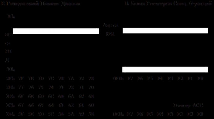
Table 1 - MCS-51 pin assignment
| Pin No. | Designation | Purpose |
| 1..8 | P1 | 8-bit quasi-bidirectional I/O port |
| 9 | RST | Reset signal (active level - high); The RST signal resets: the PC and most Special Function Registers (SFRs), disabling all interrupts and timers; selects RON Bank 0; writes "all ones" to ports P0_P3, preparing them for input; writes code 07H to the stack pointer (SP); |
| 10..17 | 8-bit quasi-bidirectional I/O port; after writing to the corresponding bit "1" - performs additional (alternative) functions: Serial port input - RxD; Serial port output - TxD; External interrupt input 0 - ~INT0; External interrupt input 1 - ~INT1; Timer/counter input 0 - T0; Timer/counter input 1 - T1; Strobe output. signal when writing to the VPD - ~ WR; Strobe output. signal when reading from the VPD - ~ RD; |
|
| 18, 19 | X1, X2 | Conclusions for connecting a quartz resonator or LC circuit; |
| 20 | GND | General conclusion; |
| 21..28 | P2 | 8-bit quasi-bidirectional I/O port; or output address A in external memory mode (VPP or VPD); |
| 29 | PME | External Program Memory read strobe, issued only when accessing external ROM; |
| 30 | ALE | External memory address strobe (VPP or VPD); |
| 31 | EA | Disabling the RPP, the level "0" at this input switches the MK to a selection of commands only from the runway ; |
| 39..32 | P0 | 8-bit bidirectional I/O port; when accessing External Memory, it issues addresses A (which are written to an external register by the ALE signal), and then exchanges a byte synchronously with the signal ~PME (for commands) or ~WR,~RD (for data in VPD), when accessing External Memory all units are written to the port register P0, destroying the information stored there; |
| 40 | Ucc | Supply voltage output |
Switching banks of RONs simplifies the execution of subroutines and handling of interrupts, because. it is not necessary to transfer the contents of the RONs of the main program to the stack when calling the subroutine (it is enough to go to another active RON bank in the subroutine).
Access to the RPD is possible using indirect or direct byte addressing (direct byte addressing allows accessing only the first 128 bytes of the RPD).
The extended RPD area (for microcontrollers of the MCS-52 family and subsequent families) from address 128 (80h) to 255 (FFh) can only be addressed using the indirect addressing method.
Table 2 - Block Registers of Special Functions (s f r)
| Mnemo code | Name | |
| 0E0h | *ACC | Battery |
| 0F0h | *B | Register battery expander |
| 0D0h | *PSW | Processor Status Word |
| 0B0h | *P3 | Port 3 |
| 0A0h | *P2 | Port 2 |
| 90h | *P1 | Port 1 |
| 80h | *P0 | Port 0 |
| 0B8h | * IP | Interrupt Priority Register |
| 0A8h | *IE | Interrupt mask register |
| 99h | SBUF | Serial transceiver buffer |
| 98h | * SCON | Serial Port Control/Status Register |
| 89h | TMOD | Timer/Counter Mode Register |
| 88h | * TCON | Timer/Counter Control/Status Register |
| 8Dh | TH1 | Timer 1 (high byte) |
| 8bh | TL1 | Timer 1 (low byte) |
| 8ch | TH0 | Timer 0 (high byte) |
| 8ah | TL0 | Timer 0 (low byte) |
| 83h | DPH | Data Pointer Register (DPTR) (high byte) |
| 82h | DPL | Data Pointer Register (DPTR) (low byte) |
| 81h | SP | Stack pointer register |
| 87h | PCON | Demand power control register |
2. SOFTWARE MODEL MCS–51


COMMAND TYPES MCS–51
Almost half of the commands are executed in 1 machine cycle (MC). With a crystal oscillator frequency of 12 MHz, the execution time for such a command is 1 μs. The remaining commands are executed in 2 machine cycles, i.e. for 2 ms. Only multiplication (MUL) and division (DIV) instructions are executed in 4 machine cycles.
During one machine cycle, there are two accesses to the Program Memory (internal or external) to read two bytes of the instruction, or one access to the External Data Memory (EDM).
3. METHODS (METHODS) OF ADDRESSING MCS–51
1. REGISTER ADDRESSING - 8-bit operand is located in the RON of the selected (active) bank of registers;
2 DIRECT ADDRESSING (indicated by the sign - #) - the operand is located in the second (and for a 16-bit operand and in the third) byte of the command;
3 INDIRECT ADDRESSING (indicated by the - @ sign) - the operand is located in the Data Memory (RPD or VPD), and the address of the memory cell is contained in one of the RONs of indirect addressing (R0 or R1); in the PUSH and POP commands, the address is contained in the stack pointer SP; the DPTR register can contain a VPD address up to 64K;
4 DIRECT BYTE ADDRESSING – (dir) – used to access RPD cells (addresses 00h…7Fh) and special function registers SFR (addresses 80h…0FFh);
5 DIRECT BIT ADDRESSING - (bit) - is used to access separately addressable 128 bits located in RPD cells at addresses 20H ... 2FH and to separately addressable bits of special function registers (see Table 3 and program model);
6 INDIRECT INDEX ADDRESSING (denoted by the @ sign) - simplifies viewing tables in the Program Memory, the PP address is determined by the sum of the base register (PC or DPTR) and the index register (Battery);
7 IMPLICIT (BUILT-IN) ADDRESSING - the instruction code contains an implicit (by default) reference to one of the operands (most often to the Accumulator).
4. PROCESSOR STATUS WORD (PSW) FORMAT

C - Carry (CARY) or borrow flag, also functions as a "boolean accumulator" in bit-operated instructions;
AC – auxiliary (additional) carry flag – set to "1" if the addition command (ADD, ADDC) had a carry from the low order tetrad to the high order (i.e. from the 3rd bit to the 4th bit);
F0 - user flag - set, reset and checked by software;
| RS1 | RS0 | Bank | Address (dir) |
| 0 | 0 | 0 | 00h..07h |
| 0 | 1 | 1 | 08h..0Fh |
| 1 | 0 | 2 | 10h..17h |
| 1 | 1 | 3 | 18h..1Fh |
RS1,RS0 – Register bank selection:
OV - Arithmetic overflow flag; its value is determined by the XOR operation of the input and output carry signals of the most significant bit of the ALU; a single value of this flag indicates that the result of an arithmetic operation in additional code out of range: –128…+127; when performing the division operation, the OV flag is reset, and in the case of division by zero, it is set; when multiplying, the OV flag is set if the result is greater than 255 (0FFH);
Bit PSW - Reserved, contains a trigger, available for writing or reading;
P - parity flag - is the addition of the number of single bits in the accumulator to an even number; is formed by a combinational circuit (programmatically available only for reading).
The MCS-51 microcontrollers do not have the "Z" flag. But in the conditional jump instructions (JZ, JNZ), the combinational circuit checks the current (zero or non-zero) contents of the Accumulator.
All commands of transfers and exchange of operands can be carried out through the Accumulator (see Fig. 3). Moreover, transfers from / to External Memory (Program Memory or Data Memory) can only be carried out through the Battery.
Most transfers can also be made via a forward byte (dir). There are even dir-to-dir transfers (see Figure 3).
Missing transfers from RON to RON can be implemented as transfers from RON to the forward byte dir (given that the RONs are located in the initial area of the Resident Data Memory, the cells of which can be addressed as dir).
XCH exchange commands allow you to send bytes without destroying both operands.
Arithmetic commands are executed only in the Accumulator. Therefore, the first operand must first be placed in the Accumulator and then add or subtract the second operand. The result is placed in the Accumulator.

The SUBB subtraction command is executed only with a borrow (i.e., the Cary flag is also subtracted from the result). Therefore, in order to execute a subtraction instruction without borrowing, it is necessary to first execute the Clear Flag C (CLRC) instruction.
The instruction for multiplying one-byte operands - MULAB - places a two-byte (16 bit) result: the low byte is in the Accumulator, the high byte is in register B.
The result of executing the instruction for dividing one-byte operands - DIVAB - is placed: the quotient - a Accumulator, the remainder - in register B.
The INC arithmetic instruction adds one to the selected operand. The DEC arithmetic instruction subtracts one from the selected operand. The Accumulator Decimal Correction (DAA) instruction helps you add binary coded decimal (BCD) numbers without converting them to hexadecimal (hex) format. The source operands must be in BCD format, i.e. in each tetrad of one byte there are only numbers from 0 to 9 (there cannot be hexadecimal numbers: A, B, C, D, E, F). Therefore, one byte can contain numbers from 00 to 99 for packed BCD numbers, or numbers from 0 to 9 for unpacked BCD numbers.
The DA A - decimal correction command performs actions on the contents of the Accumulator after adding the BCD numbers in the processor (the numbers were added according to the laws of hexadecimal arithmetic) as follows (see example):

· if the content of the low-order tetrad of the Accumulator is greater than 9 or the auxiliary carry flag is set (AC = 1), then 6 is added to the content of the Accumulator (that is, the missing six digits in hex format);
· if after that the content of the high order of the Accumulator is greater than 9 or the flag C is set, then the number 6 is added to the high order of the Accumulator.
The decimal correction instruction DA A is not used after the increment instruction (INC) because the increment instruction does not affect (change) the C and AC flags.
Logic commands:
Logical "AND" - ANL,
Logical "OR" - ORL,
The XOR logical command - XRL - is executed in the Accumulator (as well as arithmetic), but it is possible to execute logical commands also in the direct address byte (dir). In this case, the second operand can be:
in the battery or
An immediate operand in an instruction.
Rotation instructions (RR A, RL A) and rotation instructions through the CARY flag (RRC A, RLC A) rotate the contents of the Accumulator by 1 bit. Bit operands are sent only through the C flag.
Intel is the originator of the MCS-51 family architecture, which takes its name from the first representative of this family - the 8051 microcontroller, released in 1980 based on n-MOS technology. lucky set peripherals, the possibility of flexible choice of external or internal program memory and reasonable price ensured this microcontroller success in the market. From the point of view of technology, the 8051 microcontroller was a very complex product for its time - 128 thousand transistors were used in the crystal, which was 4 times the number of transistors in the 16-bit 8086 microprocessor. This microcontroller remains the core of the MCS-51 family to this day.
The main elements of the basic architecture of the family (8051 microcontroller architecture) are:
8-bit ALU;
4 banks of registers, 8 in each;
Internal (resident) program memory 4 KB, having the type ROM or EPROM (8751);
Internal (resident) data memory 128 bytes;
21 special function registers;
Boolean processor;
Two 16-bit timers/counters;
Serial port controller (UART);
Interrupt controller with two priority levels;
Four 8-bit I/O ports, two of which are used as an address/data bus for accessing external program and data memory;
Built-in clock generator.
Then the 8052 microcontroller was released, which featured an increased amount of resident program and data memory introduced by a third timer and a correspondingly expanded interrupt controller.
The next fundamental step in the development of the MCS-51 was the transfer of manufacturing technology to CMOS (modification 8xC51). This made it possible to implement the Idl (idle) and Power Down (low consumption) modes, which provide a sharp reduction in the power consumption of the crystal and opened the way for the use of a microcontroller in volatile applications, for example, in autonomous battery-powered devices.
And the last important stage in the development of the MK 8051 by Intel was the release of microcontrollers 8xC51FA / FB / FC and 8xC51RA / RB / RC, which for brevity are often referred to as 8xC51Fx and 8xC51Rx. The main distinguishing feature of this group of crystals is the presence of a specialized timer / counter (PCA). In addition, the 8xC51Rx microcontrollers additionally contain a watchdog timer (WDT). Consider the architecture and functionality of PCA in more detail.
The RSA includes:
16-bit timer/counter;
Five 16-bit sample and compare modules, each connected to a different microcontroller I/O port line.
The timer/counter serves all five sample and compare modules, which can be programmed to perform one of the following functions:
16-bit sampling of the timer value on the positive edge of the external signal;
16-bit sampling of the timer value on the negative edge of the external signal;
16-bit sampling of the timer value on any edge of the external signal;
16-bit programmable timer;
16-bit high-speed output device;
8-bit PWM.
The implementation of all the listed functions takes place in the PCA at the hardware level and does not load the central processor. This allows you to increase the overall throughput, improve the accuracy of measurements and signal processing, and reduce the response time of the microcontroller to external events, which is especially important for real-time systems. The PCA implemented in 8xC51Fx (8xC51Rx) turned out to be so
|
Designation |
Max. frequency (MHz) |
ROM/EPROM (byte) |
counters | ||
It is fortunate that the architecture of these microcontrollers has become an industry standard, and the PCA itself has been repeatedly reproduced in various modifications of the MK 8051.
Some characteristics of a number of MCS-51 microcontrollers manufactured by Intel are given in Table 1.1.
Initially, the bottlenecks of the MCS-51 architecture were an 8-bit battery-based ALU and relatively slow instruction execution (12 loops are required to execute the fastest instructions).
Table 1.1
|
I/O |
ADC inputs x digits |
periphery, peculiarities |
U pet. (IN) |
||
|
Low voltage option | |||||
|
4 levels IRQ, clock out | |||||
|
4 levels IRQ, clock out | |||||
|
Low voltage version 8xC51Fx | |||||
|
4 levels IRQ, clock out | |||||
|
4 levels IRQ, clock out | |||||
|
4 levels IRQ, clock out | |||||
clock frequency riods (MC synchronization frequency)). This limited the use of family microcontrollers in applications requiring increased performance and complex calculations (16- and 32-bit). The issue of fundamental modernization of the MCS-51 architecture has become urgent. The problem of modernization was complicated by the fact that by the beginning of the 90s a lot of developments had already been created in the field of software and hardware of the MCS-51 family, in connection with which one of the main tasks of designing a new architecture was the implementation of hardware and software compatibility with developments based on MCS-51.
To solve this problem, a joint group of specialists was created Intel companies and Philips, but the two firms later parted ways. As a result, two significantly different families appeared in 1995: Intel's MCS-251/151 and Philips' MCS-51XA (see subsection 1.2).
Key features of the MCS-251 architecture:
24-bit linear address space, addressing up to 16 MB of memory;
Register architecture that allows registers to be referred to as bytes, words, and double words;
Page addressing mode for faster fetching commands from external program memory;
Instruction queue;
Extended instruction set, including 16-bit arithmetic and logical operations;
Extended stack address space (up to 64 KB);
Execution of the fastest command in 2 cycles.
The MCS-251 instruction set includes two instruction sets - the first set is a copy of the MCS-51 instruction set, and the second consists of extended instructions that take advantage of the MCS-251 architecture. Before using the microcontroller, it must be configured, i.e. using the programmer, "burn" the configuration bits that determine which of the instruction sets will become active after power is turned on. If you install the first set of instructions, then in this case the MK of the MCS-251 family will be compatible with the MCS-51 at the binary code level. This mode is called Binary Mode. If you initially install a set of extended instructions (Source Mode), then programs written for MCS-51 will require recompilation on cross-tools for MCS-251. Source Mode allows you to use the MCS-251 architecture with maximum efficiency and achieve the highest performance.
For users focused on the use of MCS-251 microcontrollers as a mechanical replacement for MCS-51, Intel releases MCS-151 microcontrollers already programmed in the Binary Mode state.
Some characteristics of a number of MCS-251/151 microcontrollers are given in Table 1.1.
At present Intel time, aimed at the market of Pentium-processors, curtails the production of MCS-51 crystals. In general, for a particular developer, this may go unnoticed, unless he uses 8xC51GB and 80C152Jx microcontrollers, which do not have their exact analogues among products from other companies. As for all other microcontrollers of the MCS-51 family, they are all replicated many times by other companies.
The OMEVM command system provides great data processing capabilities, provides the implementation of logical, arithmetic operations, as well as real-time control. Implemented bitwise, tetrad (4 bits), byte (8 bits) and 16-bit data processing.
LSI family MCS-51 - 8-bit OMEVM: ROM, RAM, special-purpose registers, ALU and external buses have a byte organization. The two-byte data is used only by the pointer register (DPTR) and the program counter (PC). It should be noted that the data pointer register can be used as a two-byte register DPTR or as two single-byte special-purpose registers DPH and DPL. The program counter is always used as a two-byte register.
The OMEVM command set has 42 command mnemonics for specifying 33 functions of this system.
The syntax of most assembly language instructions consists of a function mnemonic followed by operands specifying addressing methods and data types. Various types data or addressing modes are determined by the set operands, not by changes in mnemonic notation.
The command system can be conditionally divided into five groups:
There are the following types of source operand addressing:
- Indirect register addressing by sum of base and index registers
Table of designations and symbols used in the command system
| Designation, symbol | Purpose |
| A | Battery |
| Rn | Registers of the currently selected register bank |
| r | The number of the loaded register specified in the command |
| direct | Directly addressable 8-bit internal data location address, which can be an internal data RAM location (0-127) or SFR (128-255) |
| @rr | Indirectly addressable 8-bit internal data RAM location |
| data8 | 8-bit immediate data included in CPC |
| dataH | MSBs (15-8) of immediate 16-bit data |
| dataL | Low bits (7-0) of immediate 16-bit data |
| addr11 | 11-bit destination address |
| addrL | Least significant bits of the destination address |
| disp8 | 8-bit signed offset byte |
| bit | Directly addressable bit whose address contains the CPC located in the internal data RAM or SFR |
| a15, a14...a0 | Destination address bits |
| (X) | The content of the X element |
| ((X)) | Content at the address stored in element X |
| (X)[M] | Discharge M element X |
+ - * AND OR XOR /X |
Operations: additions subtraction multiplication division logical multiplication (AND operation) logical addition (OR operation) addition modulo 2 (XOR) element X inversion |
Function mnemonics are uniquely associated with specific combinations of addressing methods and data types. In total, 111 such combinations are possible in the command system. The table shows a list of commands sorted alphabetically.
| Mnemonics | Function | Flags |
| ACALL team | Absolute subroutine call | |
| Addition | AC, C, OV | |
| Addition with carry | AC, C, OV | |
| AJMP team | Absolute transition | |
| Logic "AND" | ||
| Logical "AND" for variable-bits | C | |
| Compare and jump if not equal | C | |
| Team CLR A | Battery reset | |
| CLR team |
Reset bit | C, bit |
| CPL Team A | Battery inversion | |
| CPL Team |
Bit inversion | C, bit |
| Team DA A | Accumulator decimal correction for addition | AC, C |
| DEC Team<байт> | Decrement | |
| Team DIV AB | Division | C, OV |
| Team DJNZ<байт>, <смещение> | Decrement and jump if non-zero | |
| Team I.N.C.<байт> | Increment | |
| Team INC DPTR | Data pointer increment | |
| Team J.B. |
Jump if bit is set | |
| Team JBC |
Branch if the bit is set and reset this bit | |
| Team J.C. |
Jump if carry is set | |
| JMP @A+DPTR command | Indirect transition | |
| JNB Team |
Jump if bit is not set | |
| Team JNC |
Jump if no transfer is set | |
| Team JNZ |
Jump if accumulator content is non-zero | |
| Team JZ |
Jump if accumulator content is 0 | |
| LCALL Team | long call | |
| Team LJMP | long transition | |
| Forward variable-byte | ||
| Send data bit | C | |
| Command MOV DPTR,#data16 | Load data pointer with 16-bit constant | |
| MOVC instruction A,@A+( |
Move byte from program memory | |
| Send to external memory (from external memory) data | ||
● have sufficient memory capacity, its physical and logical division into program memory and data memory (Harvard architecture) and a command system oriented to the execution of control algorithms;
● include all devices (processor, ROM, RAM, I/O ports, interrupt system, bit information processing tools, etc.) microprocessor system minimum configuration controls. In the 1970s, the firm Intel developed and mastered the commercial production of a family of 8-bit MCS-48 microcontrollers, united by a number of common features (digit capacity, command system, a set of basic functional blocks, etc.). The basic version of this family includes:
● 8-bit processor;
● internal program memory (1/2/4K bytes);
● internal data memory (64/128/256 bytes);
● up to 27 internal and 16 external I/O lines;
● one 8-bit timer-counter;
● single-level interrupt system with two request sources. In 1980, the same company developed a new family of eight-bit MCS-51 microcontrollers, which is compatible with the architecture of the MCS-48 family, but has wider capabilities.
The architecture of the MCS-51 family turned out to be so successful that it is still one of the standards for 8-bit MKs to this day. Therefore, MCs of this family, which are widely used in relatively simple control systems, were chosen as the object of study.
Various program preparation tools (compilers, hardware-software emulators, etc.) have been developed for the MCS-51 family, and there are a large number of libraries of standard subroutines. The family includes various modifications of microcircuits (chip versions) of microcontrollers. The articles of this section consider in sufficient detail the basic version of microcontrollers of the MCS-51 family (8051 microcircuit corresponds to the domestic analogue KP1816BE51), the simplest in structural and functional terms and in terms of understanding.
Subsequent series of chips, while maintaining compatibility with basic version, differ from it by improved manufacturing technology, electrical parameters, additional hardware and functionality. The following articles are devoted to the structural and functional features of subsequent modifications of the MCS-51 family microcircuits.  Generalized block diagram of MCS–51. The composition of the MC, a generalized block diagram of which is shown in fig. 7.1.1, includes:
● 8-bit central processing unit CPU, consisting of ALU, control devices uu and address generator F;
● masked ROM with a capacity of 4K bytes for storing programs;
● 128 bytes RAM for data storage;
● four programmable ports Р0–Р3 for information input-output;
● BPI serial interface block for information exchange with external devices via a two-wire line;
● block of timers/counters BT/C to maintain real-time mode;
● BP interrupt block for organizing interrupts of executable programs. These funds form resident part of the microcontroller located directly on the chip. The MC includes a large number of registers, which are assigned to separate functional blocks and are not shown in the diagram.
The diagram also does not show the control circuits. Bilateral exchange of information between the blocks is carried out via an internal 8-bit data bus SD-8.
By internal 16-bit address bus SHA-16, the address formed in the CPU is displayed in the ROM (12 bits of the address) and in the RAM (8 low bits).
When using external memory, 8 low-order bits of the address are output to port P0 and 3 or 8 high-order bits are output to port P2.
For the logical extension of the interface, the combination of the functions of the port lines is used. As an example, in fig. 7.1.1 dotted line shows the lines of the port P3, performing alternative control signal transmission functions, the purpose of which will be discussed below. To create an internal clock generator, a quartz resonator and two capacitors are connected to the outputs of the microcircuit MK (Fig. 7.1.1). Instead of an internal clock generator, an external oscillator can be used for synchronization. The conventional graphic designation of the microcircuit MK is shown in fig. 7.1.2, designation and purpose of conclusions - in table. 7.1.1. Consider function blocks MK and the principle of their work.  Arithmetic-logical device. The arithmetic-logical unit is designed to perform arithmetic (including multiplication and division) and logical operations on eight-bit operands, as well as operations of logical shift, zeroing, setting, etc. The block diagram of the ALU is shown in fig. 7.1.3.
The ALU includes
● parallel eight-bit adder SM combination type with sequential transfer, performing arithmetic (addition and subtraction) and logical (addition, multiplication, disparity and identity) operations;
● battery A, providing the functions of the main arithmetic register;
● register B, used to implement the operations of multiplication and division, or as an additional super-operational register, the functions of which are defined by the user;
● registers(programmatically unavailable) temporary storageРВХ1, РВХ2, intended for receiving and storing operands for the duration of the operation;
● ROM constants ROM storing a correction code for binary-decimal data representation, a mask code for bit operations and a constant code;
● program status word register PSW, fixing the state of the ALU after the operation has been performed. In table. 7.1.2 provides information on the assignment of bits to individual digits of the PSW register. Control device. CPU Control Unit (CU) intended to coordinate the joint work of all MK nodes using the generated clock and control signals. It includes (Fig. 7.1.4): 
● synchronization and control unit USU, which generates clock pulses that set the machine cycles and their individual states (S) and phases (P), and depending on the operating mode of the MK, generates the necessary set of control signals. One, two or four machine cycles are allotted to execute the instruction.
Each machine cycle has six states S1–S6, A each state includes two phase P1, P2, the duration of which is the oscillation period of the clock generator T 0SC .
The duration of the machine cycle is 12T 0SC . All machine cycles are the same, starting with the S1P1 phase and ending with the S6P2 phase.
In addition to clock pulses, the clock device in each machine cycle generates two (sometimes one) strobe signals of the low byte of the ALE address in the form of a positive pulse in phases S1P2-S2P1 and S4P2-S5P1. Timing diagrams in fig. 7.1.5 illustrate the organization of machine cycles; 
● RK command register, command decoder DC and PLA, allowing in each machine cycle to form a set of micro-operations in accordance with the microprogram of the command being executed;
● input-output logic of LVV for receiving and issuing signals that provide information exchange between MC and external devices via ports Р0–Р3;
● The PCON register, which has a single enabled SMOD bit in position PCON.7 to double the data rate of the serial port. The remaining bits are reserved for future use.  Address generator. Address shaper (FA), or PC command counter, intended to form the current 16-bit program memory address and 8/16-bit external data memory address. It includes (Fig. 7.1.6):
● 16-bit buffer B, which communicates between the 8-bit data bus of the SD and the 16-bit internal bus (IS) of the address generator;
● SI increment scheme for increasing the value of the current program memory address by one;
● register for storing the current address of the PTA commands coming from the SI;
● Data pointer register DPTR , consisting of two 8-bit registers DPH and DPL. It serves to store a 16-bit address of the external data memory and can be used as two independent software-accessible RONs;
● RFA address generator register for storing the executive 16-bit program memory address or 8/16-bit external data memory address. This register is also used to transfer data through port P0 to external devices when executing the MOVX @Rm, A and MOVX @DPRT, A instructions.
Data memory. Data memory intended for receiving, storing and issuing information used in the process of program execution. The internal (resident) memory (Fig. 7.1.7) of data consists of RAM with a capacity of 128 bytes, stack pointer SP, address register RAM RA and decoder Dsh.  The SP stack pointer is an 8-bit register that receives and stores the address of the stack location that was last accessed. After reset, the stack pointer is set to address 07H, which corresponds to the beginning of the stack with address 08H. The address register RA together with the decoder Dsh allows access to the required memory cell containing a byte or bit of information.
The MK provides the ability to increase the amount of data memory up to 64 KB by connecting external storage devices. As an example, in fig. 7.1.8 shows the paging of external data memory VPD with a capacity of 2K bytes using instructions like MOVX @
Rm(m = 0; 1). In this case, port P0 operates as a multiplexed address/data bus, three lines of port P2 are used to address an external RAM page, and the remaining five lines can be used as I/O lines.  On fig. 7.1.9 shows the timing diagrams of read and write cycles when the MK is working with external RAM. The diagrams indicate:
● PCN - high byte of the PC command counter;
● DPL, DPH - low and high bytes of the DPTR data pointer register, which is used as an indirect addressing register in the MOVX @DPTR,A and MOVX A,@DPTR instructions;
● P2 SFR - P2 port latches;
● Rm (m = 0, 1) - registers used in MOVX @Rm, A and MOVX A, @Rm instructions as indirect address registers;
● Z - high resistance state;
● D - the period during which data from port P0 is entered into the microcontroller.  Program memory. Program memory is designed to store programs, has its own (separate from data memory) address space and is read-only. It includes a decoder Dsh and ROM (Fig. 7.1.10).
  Program memory is addressed using a 16-bit PC counter, so its maximum capacity is 64K bytes. The internal program memory consists of a ROM with a capacity of 4K bytes and a 12-bit decoder. External memory is connected according to the diagram in fig. 7.1.11.
  If 0 V is applied to the ¯EA pin of the MCU (as shown in Fig. 7.1.11), the internal program memory is disabled. All memory accesses start at address 0000h. When the ¯EA pin is connected to the power supply, the access to the internal program memory at addresses 0000h–FFFFh and to the external program memory at addresses 0FFFh–FFFFh occurs automatically.
To read the external program memory of the MK, the signal ¯PSEN is generated. When working with internal memory the read signal is not used. When accessing external program memory, a 16-bit address is always formed. The low byte of the address is transmitted through port P0 in the first half of the machine cycle and is fixed by the cut of the ALE strobe in the register. In the second half of the cycle, port P0 is used to enter a data byte from external memory into the MCU.
The high byte of the address is transmitted through the P2 port during the entire time the memory is accessed.
Timing diagrams of read and write cycles during the operation of the MK with external RAM are shown in fig. 7.1.12.  The diagrams indicate:
● PCL OUT - low byte output of the PC command counter;
● PCN OUT - issuance of the high byte of the PC command counter;
● DPH is the high byte of the DPTR data pointer register, which is used as an indirect addressing register in the MOVX @DPTR,A and MOVX A,@DPTR instructions;
● P2 SFR - P2 port latches;
● INS IN - input of instruction (command) byte from program memory;
● ADDR OUT - issuance of the low byte of the external data memory address from the Rm registers (m = 0, 1) or from the DPL register (lower register DPTR). I/O ports. Port assignment. Ports P0, P1, P2, P3 intended to exchange information between the MK and external devices, as well as to perform the following functions:
● low byte of the address А7…A0 is output through port Р0; a byte of data is output from the MK and entered into the MK when working with external program memory and external data memory (with time division);
● high byte of address A15…A8 is output through port P2 when working with external program memory and external data memory (only when using MOVX A,@DPTR and MOVX @DPTR,A commands);
● P3 port lines can be used to perform alternative functions if 1 is entered in the latch-latch of this line, otherwise 0 is fixed at the line output. Alternative functions of P3 port outputs are given in Table. 7.1.3. 
Schematic features of ports
On fig. 7.1.13 shows diagrams for one channel of each of the MK ports, including:
● a latch for fixing the received data bit;
● output amplifying cascade(driver);
● node connection with output stage (except for P2);
● a circuit for transmitting a data bit from the output side of the port, consisting of buffers B2 and B3 (for port P4). The latch is a D-flip-flop, clocked by the internal signal "Write to latch". A bit of data from the direct output of the D-flip-flop can be read by software through buffer B1 by the “Read latch” signal to the line of the internal data bus (SD) of the MK.
Output stage port P0 is an inverter, the features of which are manifested in the fact that the load transistor VT2 opens only when accessing external memory (when transferring addresses and data through the port). In all other modes, the load transistor is closed. Therefore, to use P0 (Fig. 7.1.13, a) as a general-purpose output port, external load resistors must be connected to its outputs. When writing 1 to the port latch, the inverter transistor VT1 is turned off and the external pin of the port P0.X is transferred to a high-resistance state. In this mode, the port pin P0.X can serve as an input. If port P0 is used as a general purpose I/O port, each of its P0.X pins can operate independently as an input or as an output. Output stages ports P1, P2, P3 (Fig. 7.1.13, b, c, d) made according to the circuits of inverters with an internal load resistor, which is used as a transistor VT2.
To reduce the switching time during the transition of the port outputs from state 0 to state 1, an additional transistor VT3 is introduced in parallel with the load transistor VT2. Transistor VT3 with the help of elements in the gate circuit is unlocked for a time equal to two periods of oscillation of the master crystal oscillator (during the phases S1P1, S2P2 of the machine cycle). Output stages ports P0, P2 (Fig. 7.1.13, A, c) using the MX multiplexer can be connected either to latches or to the internal buses "Address / data" and "Address". The output stage of port P1 (Fig. 7.1.13, 6) is permanently connected to the latch.
If the P3 port pin is an output and its latch contains 1, then its output stage is controlled by the hardware-internal signal “Alternative output function”, which provides the corresponding alternative function, i.e. one of the signals ¯WR, ¯RD or RxD is formed on the external pin. If the port pin is used as an input, then the alternative signal arriving at it (TxD, ¯INT0, ¯INT1, T0, T1) is transmitted to the “Alternative Input Function” internal line.
Port write mode.
When a write to port command is issued, the new value is written to the latch in phase S6P2 and output directly to the port output pin in phase S1P1 of the next machine cycle.
Port Read Mode
Port read commands read information directly from the external pins of the port pins or from latch outputs. In the first case, the data bit from the port output is read programmatically through buffer B2 by the “Read outputs” signal to the line of the internal data bus (SD) of the MK. Note that the signals "Write to latch", "Read latch", "Read pins" are generated by hardware when the corresponding commands are executed.
In the second case, the so-called "Read-Modify-Write" mode is implemented, in which the command reads the latch status signal, modifies it if necessary, and then writes it back to the latch. The Read-Modify-Write mode is implemented when the following commands are executed: ANL, ORL, XRL, JBC; CPL; I.N.C.; DEC; DJNC; MOV PX,Y; CLR PX.Y; SETB PX,Y.
Reading information from latch outputs eliminates errors when interpreting the logic level on a port pin. Read the continuation of the article in.