Low-power single-phase rectifiers. Rectifier circuits - Theoretical materials - Theory What determines the ripple frequency of the rectified voltage
Read also
2. Secondary power supplies.
Basic schemes, parameters and characteristics
2.1. Structural scheme WIEP
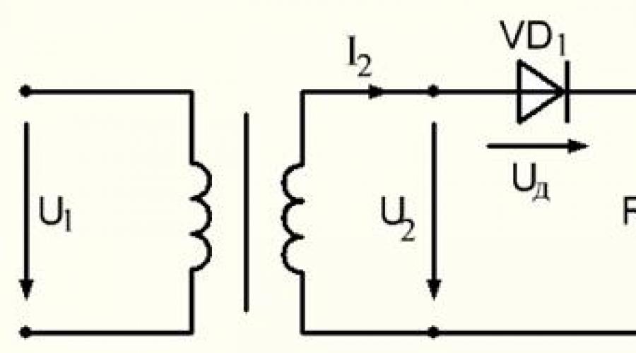
Rectifying devices convert the AC voltage of the mains into a DC voltage at the load. They are used as secondary power sources (SPS), the block diagram of which is shown in fig. 2.1.
Rice. 2.1. Structural diagram of VIEP
Power transformer Tr lowers the alternating voltage of the network U 1 frequency f=50 Hz to required value U 2. In addition, the transformer provides galvanic isolation of the power supply network and the load of the VIEP. Rectifier IN converts alternating voltage U 2 into a rectified ripple voltage of one polarity U d. Smoothing filter F reduces rectified voltage ripple U d. Stabilizer St maintains constant output voltage U out during mains voltage fluctuations U 1 or change in the load of the VIEP.
2.2.Basic rectification circuits
In low-power power supplies (up to several hundred watts), rectifiers are usually used, powered by a single-phase mains voltage. Three main diode switching circuits are used in single-phase rectifiers: a single-phase half-wave circuit on one diode, single-phase full-wave circuits: a mid-point circuit (zero circuit) on two diodes and a bridge circuit on four diodes.
DC power supplies of medium (up to 1000 W) and more (over 1000 W) power use rectifier devices powered by three-phase voltage. A three-phase rectifier can be made by an NPO in a single-half-wave circuit with three diodes or in a full-wave circuit with six diodes, which is called a three-phase bridge or Larionov circuit.
2.3. Single-phase rectifier circuits
2.3.1.Half-wave rectification circuit
A single-phase, half-wave rectification circuit (Fig. 2.2) is the simplest. semiconductor diode VD1, having one-way conduction, is connected in series with the load Rd.

Rice. 2.2. Half-wave rectification circuit
Timing diagrams (Fig. 2.3) of the rectifier voltages and currents show that in such a circuit the current i d flows through the load only during the positive half-cycle of the voltage u 2 coming from the secondary winding of the transformer (Fig. 2.3 a, b). As a result, on load Rd there is a pulsating voltage u d positive polarity (Fig. 2.3 c). In the negative half cycle voltage u 2 diode VD1 closes, current i d =0 and the diode is under the influence of reverse voltage u 2, whose maximum value is equal to the amplitude U 2 m, i.e., the voltage across the diode (Fig. 2.3 d).
Rectified ripple voltage on the load u d described by an expression in ranges, etc. and can be represented by the sum of the constant and variable components
![]()
A non-sinusoidal variable component can be represented by a series of harmonics, i.e., a series of sinusoidal components with an increasing frequency with a serial number and a decreasing amplitude. Then the pulsating voltage can be represented as a harmonic Fourier series


Rice. 2.3. Timing diagrams of a half-wave circuit
which for a half-wave rectification circuit will be written as an expression:
Using the Fourier series, the main parameters of the rectification circuit are determined.
The DC component is calculated as the average value of the rectified voltage at the load when the rectifier is in idle mode for the period of the mains voltage
The average value of the pulsating current in the load is determined by the expression: .
The variable component of the rectified voltage is characterized by its maximum value (fundamental harmonic): , where ![]() is the amplitude of the fundamental harmonic.
is the amplitude of the fundamental harmonic.
The efficiency of the rectifier is determined by the value of the ripple factor, which is determined by the ratio of the amplitude of the fundamental harmonic U m to the average value of the rectified voltage
![]()
In this case, the ripple frequency of the main harmonic coincides with the ripple frequency of the rectified voltage and is equal to the mains voltage frequency: ![]()
The advantage of a half-wave circuit is simplicity. Disadvantages: large dimensions of the transformer, high ripple factor, low frequency main harmonic. Therefore, such a rectification circuit is of limited use, mainly for supplying low power and high voltage circuits, for example: cathode ray tubes.
2.3.2.Full-wave circuit with mid-point
A single-phase full-wave circuit with a midpoint (Fig. 2.4) is parallel connection two half-wave rectifiers, the diodes of which work on a common load.

Rice. 2.4. Full-wave circuit with mid-point
When voltage is applied u 1 voltages appear on the primary winding of the transformer on each half of the secondary winding u 21, u 22(Fig. 2.5 a). Secondary windings W 21 And W 22 included in sequence and according to. The diodes of the circuit conduct current alternately, each for a half-cycle (Fig. 2.5 b, c). In the first half ![]() to the diode VD1 positive voltage half wave applied u 21, in the circuit diode - winding W 21 current flows i 21(see Fig. 2.5 b). Diode VD2 at this time it is closed, since to it through the diode open at this time VD1 reverse voltage applied to both windings of the transformer
to the diode VD1 positive voltage half wave applied u 21, in the circuit diode - winding W 21 current flows i 21(see Fig. 2.5 b). Diode VD2 at this time it is closed, since to it through the diode open at this time VD1 reverse voltage applied to both windings of the transformer ![]() (Fig. 2.5 e). In the next half
(Fig. 2.5 e). In the next half ![]() the diode will open VD2, and current i 22 will flow through the circuit diode - winding W 22. (see Fig. 2.5 c). Thus, through the load resistance Rd currents flow alternately in the same direction i 21 And i 22. As a result, on load Rd half-waves of current are formed i d and stress u d of the same sign (Fig. 2.5 d, e).
the diode will open VD2, and current i 22 will flow through the circuit diode - winding W 22. (see Fig. 2.5 c). Thus, through the load resistance Rd currents flow alternately in the same direction i 21 And i 22. As a result, on load Rd half-waves of current are formed i d and stress u d of the same sign (Fig. 2.5 d, e).
The voltage rectified by this circuit, like the voltage of a half-wave circuit, is pulsating, that is, it can be decomposed into a harmonic Fourier series.
Where is the average value of the rectified voltage at the load. When the rectifier is in idle mode, it is determined by the expression:

Rice. 2.5. Timing Diagrams for Midpoint Circuit
Hence the effective value of the voltage in the secondary winding of the transformer:
![]()
The amount of rectified current I d is defined by the expression:
![]()
Amplitude of current in the secondary winding of the transformer ![]() and the effective value
and the effective value ![]() .
.
In the two-half-wave circuit, the amplitude of the main harmonic component decreased to the value , and consequently, the ripple coefficient also decreased:
![]() .
.
From the timing diagrams (see Fig. 2.5 a, e) it can be seen that the voltage on the load reaches its maximum value U 2 m twice per period of rectified voltage. Therefore, the load voltage ripple frequency U d equal to twice the mains voltage frequency:
In a rectification circuit with a midpoint, the currents in the secondary windings flow alternately (in the winding W 21 from end to beginning, and in the winding W 22 from end to end), so the transformer core is not magnetized and a pure sinusoidal current acts in the primary winding, which leads to a decrease in typical power and best use transformer. Compared to the half-wave rectification circuit, the value of the rectified voltage has doubled U d and current I d, the ripple coefficient has decreased.
Disadvantages of the circuit: the need to output the midpoint of the secondary winding, the need to balance the secondary windings to ensure equality, a large reverse voltage across the diodes, an increase in the dimensions of the transformer.
2.3.3.full wave bridge
In the circuit under consideration (Fig. 2.6), the rectifier consists of four semiconductor diodes, assembled according to the scheme of the bridge, in one of the diagonals of which ab the voltage of the secondary winding of the transformer is connected, and in the other cd– load resistance Rd. The positive pole of the load is the common connection point of the cathodes of the diodes (point d), negative - the connection point of the anodes (point With).

Rice. 2.6. full wave bridge
The operation of the circuit is shown in fig. 2.7, which shows the forms of currents and voltages for an idealized bridge circuit in its various sections. The voltage and current of the secondary winding of the transformer change over time according to the harmonic law (Fig. 2.7a)
![]() ;
; ![]()
In the positive half cycle of the supply voltage ![]() point potential A is positive, and the points b- negative. Diodes VD1 And VD3 will be included in the forward direction and the current pulse i 13 will pass from the positive terminal of the secondary winding through the diode VD1, load Rd and through an open diode VD3 to the negative terminal of the secondary winding of the transformer (Fig. 2.6). The shape of this current will repeat the shape of the current i 2 secondary winding of the transformer (Fig. 2.7b). Passing through the load Rd, current pulse i 13 puts stress on it u d(Fig. 2.7d), which, without taking into account the voltage losses on the diodes, repeats the shape of the positive voltage half-wave, i.e., has a ripple amplitude During the first half-cycle, the diodes VD2 And VD4 are locked because they are turned on in the opposite direction. These diodes are subjected to a negative reverse voltage, the maximum value of which
point potential A is positive, and the points b- negative. Diodes VD1 And VD3 will be included in the forward direction and the current pulse i 13 will pass from the positive terminal of the secondary winding through the diode VD1, load Rd and through an open diode VD3 to the negative terminal of the secondary winding of the transformer (Fig. 2.6). The shape of this current will repeat the shape of the current i 2 secondary winding of the transformer (Fig. 2.7b). Passing through the load Rd, current pulse i 13 puts stress on it u d(Fig. 2.7d), which, without taking into account the voltage losses on the diodes, repeats the shape of the positive voltage half-wave, i.e., has a ripple amplitude During the first half-cycle, the diodes VD2 And VD4 are locked because they are turned on in the opposite direction. These diodes are subjected to a negative reverse voltage, the maximum value of which ![]() (Fig. 2.7e).
(Fig. 2.7e).
When there is a change in the polarity of the voltage on the secondary winding of the transformer, while the anode of the diode VD2 connects to "+", and the cathode of the diode VD4 to "-" voltage (see Fig. 2.6). Now during the second half-cycle ![]() under direct voltage
under direct voltage


Rice. 2.7. Bridge Timing Diagrams
be diodes VD2 And VD4, and the diodes VD1 And VD3 locked by reverse voltage ![]() (see Fig. 2.7g).
(see Fig. 2.7g).
In the circuit of the secondary winding of the transformer, open diodes VD2 And VD4 and loads Rd a current pulse will pass i 24(see Fig. 2.7c) the same shape as the current pulse i 13, releasing a voltage pulse on the load, the magnitude and polarity of which is the same as in the first half-cycle (Fig. 2.7e).
Thus, for the period of the converted voltage in the load circuit Rd two current pulses pass without changing their direction and creating a load current ![]() (see Fig. 2.7d), under the influence of which a pulsating voltage is generated on the load (see Fig. 2.7e), of the same type as for a circuit with a midpoint. The rectified voltage contains a constant component and an infinite number of harmonic components and can be written as a harmonic Fourier series:
(see Fig. 2.7d), under the influence of which a pulsating voltage is generated on the load (see Fig. 2.7e), of the same type as for a circuit with a midpoint. The rectified voltage contains a constant component and an infinite number of harmonic components and can be written as a harmonic Fourier series:
The DC component is calculated as the average value of the rectified voltage at the load when the rectifier is in idle mode:

![]()
When calculating the rectified current I d through the load, it should be taken into account that when current passes through an open diode, voltage drops on it, the value of which is indicated in the reference books, therefore, the current in the load is determined by the expression:
![]()
The current value of the secondary winding current is related to the load current by the relation: The main harmonic component of the rectified voltage is determined by the expression:
![]()
therefore, the ripple frequency is equal to twice the frequency of the converted mains voltage:
The amplitude of the main harmonic component has decreased compared to the one-half-wave circuit, and therefore the ripple factor has also decreased:
![]() .
.
In order to prevent damage to diodes during their operation in rectification circuits, it is necessary to take into account the maximum values of voltage and current in the secondary winding of the transformer when choosing diodes. The maximum reverse voltage across the diode is equal to the voltage at the ends of the secondary winding. Therefore, for circuits with a midpoint ![]() , and for half-wave and bridge circuits -
, and for half-wave and bridge circuits - ![]() . In full-wave rectification circuits, the current pulse passes through the diode only during a half-cycle, therefore, the average value of the current flowing through the diode is half the rectified current: In a half-wave circuit, the same current flows through the diode and the load:
. In full-wave rectification circuits, the current pulse passes through the diode only during a half-cycle, therefore, the average value of the current flowing through the diode is half the rectified current: In a half-wave circuit, the same current flows through the diode and the load:
The bridge circuit is the basic circuit for single-phase rectifiers. It can be used without a transformer, that is, it can be connected directly to the circuit alternating current, if the mains voltage provides the required value of the rectified voltage. When working with a transformer, current pulses i 13 And i 24 in the secondary winding of the transformer, they are directed towards each other, so their constant components are compensated, and the transformer operates in a mode without constant bias. Compared to the mid-point circuit, the bridge circuit has a smaller transformer size, since only one winding is placed on the secondary side.
2.4.Smoothing filters
The voltage at the output of any block of diodes is always pulsating, containing, in addition to the constant voltage, a number of sinusoidal components of different frequencies. In most cases food electronic devices pulsating voltage is completely unacceptable. The requirements for the permissible value of the ripple coefficient depend on the purpose and mode of operation of the device. For example, for input amplifier stages, the ripple factor can be in the range ![]() . To power devices, these ripples must be reduced to a minimum level at which they do not significantly affect the operation of electrical devices.
. To power devices, these ripples must be reduced to a minimum level at which they do not significantly affect the operation of electrical devices.
For this purpose, smoothing filters are used, which pass only the direct component of the rectified voltage to the output and attenuate its variable components as much as possible. The main elements of the filters are inductance (connected in series with the load) and capacitor (connected in parallel with the load). The smoothing effect of these elements is due to the fact that the inductance represents a large resistance () for currents high frequency and small for low frequency currents, and the capacitor has a large resistance (for low frequency currents and low resistance for high frequency currents.
The efficiency of ripple smoothing is estimated by the smoothing coefficient, which is the ratio of the ripple coefficient at the input and output of the filter
The smoothing coefficient shows how many times the filter reduces the ripple of the rectified voltage.
Depending on the method of switching on the capacitor and inductance, the following types of filters are distinguished: capacitive (Fig. 2.8 a), inductive (Fig. 2.8 b), L-shaped (Fig. 2.8 c), L-shaped (Fig. 2.8 d).

Rice. 2.8. Wiring diagrams for smoothing filters
On fig. 2.9 shows waveforms of the output voltages of a full-wave rectifier when operating without a filter (Fig. 2.9 a), when capacitive (Fig. 2.9 b) and inductive (Fig. 2.9 c) filters are turned on.

Rice. 2.9. Time diagrams during operation: a) without filter;
b) with a capacitive filter; c) with inductive filter
When using a capacitive filter, the smoothing of the ripple of the rectified voltage and current occurs due to the periodic charging of the capacitor and its subsequent discharge to the load resistance. The capacitor is charged by current i d flowing through the diode for a short period of time, when the instantaneous value of the pulsating voltage at the rectifier output (Fig. 2.9 a) is higher than the voltage at the load (and at the capacitor). The time constant of the capacitor charge is determined by the capacitance of the filter capacitor and a small resistance equal to the sum of the direct resistance of the open diodes and the active resistance of the transformer reduced to the secondary winding. When the voltage becomes less than the voltage across the capacitor, the diodes close and the capacitor is discharged through the load resistance (Fig. 2.9 b). With a large capacitor capacitance and load resistance, the time constant for discharging the capacitor is much greater than the time constant for charging it. In this case, the discharge of the capacitor proceeds in time almost according to a linear law, and the output voltage (Fig. 2.9 b) does not decrease to zero, but pulsates within certain limits. increasing the average value of the rectified voltage , which can reach the maximum value ![]() with a large capacitor.
with a large capacitor.
For effective work smoothing filter, the capacitance at the frequency of the fundamental harmonic must be at least an order of magnitude less than the load resistance:
![]()
It follows that the use of a capacitive filter is more efficient for high-resistance loads with low rectified currents, since this increases the efficiency of smoothing.
When switched on in series with the load of an inductive filter (Fig. 2.8 b), a changing magnetic field excited by a pulsating current induces an electromotive force of self-induction. In accordance with the Lenz principle, the electromotive force is directed in such a way as to smooth out the current ripples in the circuit, and, consequently, the load voltage ripples (Fig. 2.9 c). Smoothing efficiency increases at high values of the rectified current.
The value of the filter inductance is chosen in such a way that the inductive reactance is significantly greater than the value of the load resistance.
A greater reduction in the ripple of the rectified voltage is provided by mixed filters that use capacitors and inductances, for example, L-shaped smoothing filters (Fig. 2.8 c, d). However, when using these filters, the value of the direct component of the rectified voltage at the load decreases due to the drop in part of the voltage across the active resistances of the inductor winding or.
2.5.External characteristic of the rectifier
The external characteristic determines the boundaries of the change in load current, at which the rectified voltage at the load does not decrease below the permissible value when the load resistance changes. The external characteristic is described by the equation:
where is the average value of the rectified voltage in the idle mode of the rectifier, is the active component of the resistance of the transformer windings, is the voltage drop across the diodes of one rectifier arm. For a circuit with a midpoint , for a bridge - , - voltage drop across an open diode.
External characteristic 1 (Fig. 2.10) corresponds to a rectifier without a filter, characteristic 2 - to a rectifier with a capacitive filter, and when an L-shaped LC filter is included in the circuit, characteristic 3 is obtained. the capacitor charge count can rise to a maximum value.

Rice. 2.10. External characteristics of the rectifier
The decrease in output voltage with increasing load current is explained by the voltage drop across the circuit elements: resistance and diodes. When the capacitive filter is turned on, an additional decrease in the output voltage occurs due to a faster discharge of the capacitor to a lower load resistance. When the L-shaped LC filter is turned on, an additional decrease in voltage at the load is caused by a voltage drop across the connected inductive filter in series.
2.6. Three-phase rectifier circuits
2.6.1. Three-Phase Mid-Point Rectifier
A three-phase rectification circuit with a midpoint (Fig. 2.11) is also called a three-phase single-cycle circuit, since only one of the half-waves is rectified AC voltage each phase. The three-phase rectification circuit includes a transformer, the primary windings of which can be connected in a star or delta, and the secondary windings can only be connected in a star. ends a, b, c secondary windings of the transformer are connected to the anodes of three diodes VD 1, VD 2, VD 3. The cathodes of the diodes are connected together and serve as the positive pole for the load circuit, and the transformer midpoint terminal is the negative pole.

Rice. 2.11. Rectification scheme
Operation of the rectifier on an active load.
Initially, we assume that the load of the rectifier circuit is active, i.e. X d= 0. For simplicity, we will consider the diodes and the transformer to be ideal, i.e. the resistance of the diode in the forward direction is zero, and in the reverse direction it is infinitely large, the active resistance and leakage inductance Xa windings of the transformer and the inductance of the supply network are taken equal to zero. Then the transition of current from one diode to another is considered instantaneous. The operation of the circuit is illustrated by the diagrams shown in fig. 2.12. From the timing diagram (see Fig. 2.12 a) it can be seen that the voltages u 2 a, u 2 b , u 2 c phase shifted by one third of the period (2p/3) and during this interval the voltage of one phase is higher than the voltage of the other two phases relative to the zero point of the transformer. The diodes of the circuit operate alternately in 1/3 cycles (2p/3). At some point in time, that diode conducts current, the potential of the anode of which in relation to the zero point of the transformer is higher than that of other diodes. This is true for the case of connecting diodes into a cathode group. The current in each diode flows for 1/3 of the period (2p/3) and stops when the anode potential of the working diode becomes lower than the potential of the cathodes. The diode closes and a reverse voltage is applied to it. u b(see Fig. 2.12 c). The transition of current from one diode to another occurs at the moment of intersection of the phase voltage curves (points a, b, c, d in Fig. 2.12a). Rectified current i d goes through the load Rd continuously and consists of alternating anode currents i a 1 ,i a 2 , i a 3 . Instantaneous value of the rectified voltage u d(see Fig. 2.12b) at each moment is determined by the instantaneous value of the voltage of the phase to which the working diode is connected. Rectified voltage u d represents the envelope of the sinusoids of the phase voltages u 2 secondary windings of transformer T. Rectified current curve i d at Xa = 0, X d= 0 repeats the rectified voltage curve. Current waveform i a in diode VD 1 is shown in fig. 2.12c. diode current VD 1 in this case will also be the current i 2 a secondary winding of the transformer. Reverse voltage curve u b 1 on diode VD 1 is formed from sections of sinusoids of linear voltages ( u ab, u with a), because the anode of the idle diode is connected to one of the phases, and the cathode, through an open diode, to the other phase of the secondary winding. The instantaneous values of the phase-to-phase (line-to-line) voltage correspond to the ordinates of the area shaded in fig. 2.12a. Based on them, a linear diagram of the reverse voltage is built. u b 1, on a diode VD 1 (see Fig. 2.12 c).  S T = = 1,345P d,
Where S 1 = 3U 1 I 1 = 1,21P d- calculated power of the primary winding of the transformer;
S 2 = 3U 2 I 2 = 1,48P d- calculated power of the secondary winding of the transformer;
P d = U d I d- power in the load.
In a three-phase rectifier with a midpoint, the phenomenon of forced magnetization of the transformer magnetic circuit takes place, since. currents of the secondary windings of the transformer i 2 a,i 2 b, i 2 c contain a constant component equal to I d , which creates a unidirectional flux of forced magnetization of the transformer in each core of the magnetic circuit. This flow, pulsing at a triple frequency with respect to the frequency of the supply network, closes partly through the core, partly through the air and steel reinforcement surrounding the transformer core, causing them to heat up. As a result, the transformer core is saturated, and heat losses occur in the steel reinforcement due to eddy currents induced by the variable component of the forced magnetization flux. Saturation of the transformer magnetic circuit leads to a sharp increase in the magnetizing current (no-load current) of the transformer. In order to avoid saturation, it is necessary to increase the cross section of the magnetic circuit. However, this leads to an overestimation of the weight and size parameters of the transformer and the entire rectifier installation. To eliminate additional losses caused by the variable component of the forced magnetization flux, the primary windings of the transformer must be connected in a "triangle". In this case, only the constant component remains in the forced magnetization flux; the variable component with a pronounced third harmonic is compensated by flows that create higher harmonic currents with a frequency that is a multiple of three, contained in the currents of the primary windings of the transformer and closing along the circuit formed by these windings. The calculated power of the transformer when connecting the windings with a "triangle" does not change.
2.6.2.Three-phase bridge
A significant number of three-phase current rectifiers are carried out according to a bridge circuit (Larionov's circuit), containing a three-phase transformer and a rectifier unit of six diodes (Fig. 2.13.) The primary and secondary windings of the transformer can be connected in a star or triangle circuit. However, the bridge rectification circuit can be used without a transformer. Diodes in the rectifier unit are divided into two groups:
1) cathode, or odd (diodes VD 1, VD 3, VD 5), in which the cathodes of the diodes are electrically connected and their common terminal is a positive pole for the external circuit, and the anodes are connected to the terminals of the secondary windings of the transformer;
2) anode, or even (diodes VD 2, VD 4, VD 6), in which the anodes of the diodes are electrically connected to each other, and the cathodes are connected to the anodes of the first group. The common anode connection point is the negative pole for the external circuit. The load is connected between the connection points of the cathodes and anodes of the diodes.
A three-phase bridge circuit can be represented as a series connection of two three-phase circuits with a midpoint fed from one winding of a transformer. At any moment in the cathode group, the diode will be opened, the anode potential of which is higher than the anode potentials of other diodes in the cathode group, and in the anode group, the diode, the cathode potential of which is lower than the potentials of the cathodes of other diodes of the anode group.

Rice. 2.13. Rectification scheme
The operation of the circuit can be traced using the timing diagrams in Fig. 2.14. Since the operating modes of the circuit for active and active-inductive loads differ slightly, we will analyze the operation of the circuit for the most common active-inductive load, taking X a = 0, X d = 0. The diodes of the cathode group open at the moment of crossing the positive sections of the phase voltage curves (points a, b, c, d, e in Fig. 2.14a), and the diodes of the anode group - at the moment of crossing the negative sections of the phase voltage curves (points k, l , m, n). Each diode is open for one third of the cycle. With instantaneous switching of current in a three-phase bridge circuit, at any time, current is carried on
Answers to security questions lab №1
What are the advantages of a full wave rectifier circuit over a single half wave?
First, the current passes through secondary winding transistor during each half-cycle in different directions.
Secondly, the ripple frequency is twice as high and equal to 100 Hz, since during the period of the mains voltage, the current in the load and the voltage across it reach a maximum twice.
Thirdly, its output impedance is half that.
Fourthly, the ripple coefficient is less and equal to 0.67.
What is the advantage of a bridge rectifier circuit over a full wave rectifier circuit?
Diodes can be designed for half the reverse voltage, since it is equal to the amplitude of the alternating voltage on the secondary winding.
Draw a bridge rectifier circuit with a smoothing filter and show the current flow paths.
Compare the properties of smoothing LC and RC filters.
feature LC-filters are low losses, allowing them to be used in devices with a relatively large load current. In low-power rectifiers (current up to 10-15 mA) can be used RC-filters. Their disadvantage is low efficiency.
Why can diodes be connected in series in rectifiers?
The series connection of rectifier diodes is done when it is necessary to increase the total allowable reverse voltage applied to each of them.
Why, when semiconductor diodes are connected in series in a rectifier, are they shunted with resistors?
The reverse resistances of rectifier diodes have a large spread (the differences reach up to one or two orders of magnitude), so the reverse voltage applied to the circuit of series-connected diodes will be distributed unevenly, but in proportion to their reverse resistances. The largest voltage drop will be on the diode with a large reverse resistance. This can lead to electrical and then thermal breakdown. r-p transition of this diode; after that, the reverse voltage is distributed among the remaining diodes. There will be a breakdown of the next diode, which has the highest reverse junction resistance among the remaining diodes. And so one by one the diodes will fail. To prevent this from happening, you should equalize the reverse voltage drops on the diodes of the series chain by shunting them with resistors of the same resistance. The resistance of the shunt resistor is selected large to eliminate large power losses on it.
What is the filter smoothing coefficient and how does its value depend on the capacitance of the filter capacitors and the load current.
An important characteristic of filters is the smoothing coefficient - , where: - ripple coefficient at the filter input, - ripple coefficient at the filter output.
With an increase in the load current, the amplitude of the ripples at the output of the capacitive filter increases, and the inductive filter decreases. Therefore, it is advantageous to use a capacitive filter at low load currents, and an inductive filter at high load currents. Increasing the capacitance of the capacitor reduces the amplitude of the ripple.
With what frequency does the voltage on the load pulsate in the case of a half-wave rectifier, a full-wave one?
In the case of a half-wave rectifier, the voltage ripple frequency at the load is equal to the input ripple frequency (50 Hz), a full-wave rectifier is twice as high (100 Hz).
What is the function of the capacitors C 1 , C 2 and the inductor in the smoothing filter?
Capacitors are used to smooth out voltage ripples, and chokes so that the capacitances of these capacitors do not add up.
Give an example of a voltage multiplication circuit.
Voltage doubling circuits:
How does the capacitance of the filter capacitors and the load resistance affect the amplitude of the ripple?
With an increase in the load current, the amplitude of the ripples at the output of the capacitive filter increases, and the inductive filter decreases. Increasing the capacitance of the capacitor reduces the amplitude of the ripple.
Why does the inductor poorly smooth out ripples at the rectifier output at low load current?
With an increase in the load current, an increase in the energy accumulated in the inductor occurs, while the self-induction EMF increases, which prevents the variable current component from passing into the load. This improves the smoothing properties of the filter.
Answers to security questions lab#5
1. When the transistor is turned on, the input resistance of the amplifying stage is the smallest?
Scheme with Common Base.
2. When turning on the transistor, the amplifying stage has the highest input resistance?
Scheme with a common collector.
3. What amplifier is called an emitter follower? What are its purposes, properties?
Amplifier OK. An emitter follower is needed to provide a large input impedance to the amplifier.
4. Explain the purpose of the elements included in the circuit of a resistive-capacitive transistor amplifier.
The circuit R B1 and R B2 is a voltage divider of a DC source. It is needed to supply voltage to the base, with the help of which the base current is set and thereby the position of the operating point on the static current-voltage characteristics of the transistor is set.
R K - load resistor. DC sets the collector voltage, which determines the position of the operating point of the transistor. Variable is the load of the amplifier.
R E is the resistor for temperature stabilization of the position of the operating point of the transistor
C E - eliminates negative feedback on alternating current.
С Р - separating capacitors. .
5. How the transistor is biased p-n-p type when it is turned on according to the scheme with a common emitter?
In the circuit with OE, the DC mode of the transistor is created by: elements R E, C E - temperature stabilization circuit; R B1, R B2 - a divider that creates a bias voltage at the base. Bias by a fixed voltage gives good results when replacing the transistor and changing the temperature. However, it is not economical due to the loss of part of the energy of the power source in the voltage divider R B1 , R B2 .
6. What is the active mode of the transistor?
Working in active mode, the transistor amplifies the electrical signal. You can get this mode by turning on the emitter junction in the forward direction, and the collector junction in the opposite direction.
7. What happens to the operating point of the transistor when the resistance of the resistors R B1 and R B2 changes?
When the resistance of the resistors R 1 and R 2 changes, the operating point shifts.
8. How will the gain of the cascade (circuit with OE) change if the capacitor C E is excluded from it?
The cascade stops amplifying the signal.
9. What elements of the circuit affect the frequency response of the amplifier in the region of low and high frequencies of the signal?
In the low-frequency region, distortions depend on the separating capacitance C R. The decrease in the frequency response in the high-frequency region is due to the load capacitance, if any.
10. How do non-linear distortions manifest themselves when amplifying sinusoidal signals?
Nonlinear distortion arise due to the fact that the current-voltage characteristics of transistors are not linear. As a result, signals appear in the amplifiers that were not at the input of the amplifier, the frequencies of these signals are multiples of the frequency of the input signal and are called harmonics. The harmonic number is integer and its amplitude is usually inversely proportional to their number.
Answers to security questions lab №3
What is the difference between intrinsic and extrinsic electrical conductivity of semiconductors?
Intrinsic conductivity arises as a result of the transition of electrons from upper levels valence band to the conduction band.
Impurity conductivity arises if some atoms of a given semiconductor are replaced at the sites of the crystal lattice by atoms whose valency differs by one from the valence of the main atoms. In contrast to the case considered above, the formation of a free electron is not accompanied by the breaking of covalent bonds, i.e., the formation of a hole.
Describe the occurrence and properties p-n transition.
p-n junction is a thin layer at the boundary between two regions of the same crystal. To make such a transition, for example, a single crystal of very pure germanium with an electronic conduction mechanism is taken. A piece of indium is melted into a thin plate cut from a crystal on one side. During this operation, which is carried out in a vacuum or in an inert gas atmosphere, indium atoms diffuse into germanium to a certain depth. In the region into which indium atoms penetrate, the conductivity of germanium becomes hole. A p-n junction occurs at the boundary of this region. There are other ways getting p-n transitions.
Describe the device and principle of operation of a bipolar transistor in a circuit with a common emitter.
The transistor, or semiconductor triode, being a controlled element, has found wide application in amplification circuits, as well as in pulse circuits. Lack of heat, small dimensions and cost, high reliability.
A bipolar transistor is a three-layer semiconductor structure with alternating electrical conductivity layers and contains two p-n junction. And of course there are p-n-p and n-p-n transistors. Germanium and silicon are used as the starting material for obtaining a three-layer structure.
Draw and explain the type of input and output characteristics of the transistor when it is turned on according to the circuit with a common emitter.
A) The family of input characteristics () at At the input CVC has the form of a direct CVC branch of the electron-hole junction, since the emitter junction (EC) and the collector junction (CC) are forward-biased and connected in parallel to each other (and the internal resistance of this emf is zero. At the input I–V characteristic is shifted to the right due to the additional voltage drop across the EA from the collector current flowing through the transistor. This voltage drop exists even in the absence of base current and corresponds to the “o-a” section
B) The family of output characteristics () at is shown in fig. 14.2, b. At , the output I–V characteristic has the form of the reverse branch of the I–V characteristic of the electron-hole transition, increased by () times (where is the current transfer coefficient), since the CP is shifted in the opposite direction. With an increase in the base current, the output I–V characteristics are shifted up by .
What other wiring diagrams are available bipolar transistor? List their main properties.
The OK circuit has the largest input resistance and the smallest output resistance compared to other transistor switching circuits. The amplifier in this circuit does not amplify in voltage.
The OB circuit has the smallest input resistance and the largest output resistance compared to other transistor switching circuits.
List and explain the physical meaning of the h-parameters of the transistor. How to determine them from static characteristics?
![]() input impedance, at short circuit output circuit ;
input impedance, at short circuit output circuit ;
![]() voltage feedback factor, at no-load in the input circuit. Characterizes the internal feedback between the input and output circuits of the transistor;
voltage feedback factor, at no-load in the input circuit. Characterizes the internal feedback between the input and output circuits of the transistor;
![]() current transfer coefficient at which the output circuit is closed;
current transfer coefficient at which the output circuit is closed;
![]() output conductance, at idle in the input circuit
output conductance, at idle in the input circuit
How does the coefficient h 21e change when h 21b changes?
The closer h 21b to one, the greater h 21e.
Why can a common-emitter transistor provide current gain?
The value is the main parameter that determines the amplifying properties of a bipolar transistor. , since , then the transistor connected according to the scheme with OE amplifies the signal.
Why is the input resistance of a transistor in a common emitter circuit greater than in a common base circuit?
Unlike the circuit with OE, in the circuit with OB the input signal is fed to the emitter junction, which is connected in the forward direction and does not prevent the flow of current.
Why is the value of h 21e greater than 1?
Because .
What electrical parameters characterize the position of the operating point on the static characteristics of the transistor?
What are the features of the active mode of operation of the transistor? What other modes of operation of the transistor do you know?
Working in active mode, the transistor amplifies the electrical signal.
Saturation - can be obtained by turning on both p-n junctions in the forward direction.
Cutoffs - can be obtained by turning on both p-n junctions in the opposite direction.
Conclusion: I investigated the static characteristics of a bipolar transistor in a common emitter circuit and the definition of its main parameters. In exercise 1 with
U KE, B=0 the graph at the end deviated upwards from other values.
Control questions No. 1-C
Define the basic logical operations and, or, not.
Disjunction(OR) is a complex logical expression that is true if at least one of the simple logical expressions is true and false if and only if both simple logical expressions are false.
Designation: F = A + B.
Conjunction(s) is a complex logical expression that is considered true if and only if both simple expressions are true, in all other cases, this combined expression is false.
Designation: F = A & B.
Inversion (NOT, denunciation) is a complex logical expression, if the original logical expression is true, then the result of the negation will be false, and vice versa, if the original logical expression is false, then the result of the negation will be true. Others simple words, this operation means that to the original boolean expression the particle NOT is added or the words WRONG WHAT
On what elements can the basic logical functions be implemented?
With the help of only one elements OR - NOT or only elements AND - NOT, by various inclusions of them with each other, you can perform any logic function.
Develop diagrams of electromechanical analogues of devices for the implementation of logical functions AND. OR, NOT, 2AND-NOT, 2OR-NOT.
What are the advantages of integrated logic circuits?
The advantages of ICs are high reliability, small size and weight.
Chips are economical and reduce power consumption and weight of the IP
Integrated circuits are inertialess.
Draw the integrated circuit of the basic TTL element and explain its operation.
The basis of transistor-transistor logic is a base element based on a multi-emitter transistor T1, which is easily implemented in a single technological cycle with a transistor T2. In TTL logic, a multi-emitter transistor performs an AND operation in positive logic, and an inverter is assembled on transistor T2. Thus, according to this scheme, the AND–NOT basis is implemented.
If a high potential is applied to all inputs of the circuit, all the emitter-base transitions of the transistor T1 will turn off, since the potential at point A is approximately equal to the input signals. At the same time, the base-collector junction will be open, therefore, the current Ib us flows through the circuit Ep - R1 - base T1 - collector T1 - base T2 - emitter T2 - case, which opens the transistor T2 and introduces it into saturation. The potential at the output of the circuit turns out to be close to zero (at the level of ≈ 0.1 V). The resistance R1 is chosen so that, due to the voltage drop across it from the current Ib of the transistor T2, the potential at point A would be lower than the potential of the inputs, and the emitters of T1 would remain locked.
When a low potential of a logical zero is applied to at least one of the inputs, this emitter-base transition of the transistor T1 opens, a significant current Ie appears and the potential at point A, equal, approaches zero. The potential difference between the base and emitter T2 also becomes equal to zero, the current Ib of the transistor T2 stops, and it closes (turns into cutoff mode). As a result, the output voltage acquires a value equal to the supply voltage (logical unit).
A significant disadvantage of the considered circuit of the AND-NOT element is the low load capacity and efficiency of its inverter, therefore, in practical circuits, a more complex inverter is used.
To reduce the voltage ripple at the consumer, a special device is installed at the rectifier output, called a smoothing filter, the main purpose of which is to reduce the variable component of the rectified voltage. The simplest filter is a large capacitor connected in parallel to the rectified voltage receiver. With this inclusion, the capacitor is charged to the amplitude value of the voltage u 2 at times when the voltage u 2 exceeds the voltage on the capacitor (time interval t 1 -t 2 in Fig. 6.7). During the time interval t2-t3 when the voltage u c u 2 , the valve is closed and the capacitor is discharged through the load resistor R n. From the moment of time t3 the process is repeated. When the capacitive filter is turned on, the voltage u n does not decrease to zero, but pulsates within certain limits, increasing the average value of the rectified voltage.
A greater reduction in voltage ripple is provided by L-shaped filters, which are mixed LC filters (Fig. 6.8). Ripple reduction LC filter is explained by the shunting action of the capacitor C f for the variable component of the rectified voltage and a significant drop in this voltage component on the coil L f, which is called a throttle. As a result, the proportion of the variable component in the rectified voltage is sharply reduced. Along with the weakening of the variable component of the rectified voltage LC the filter also slightly reduces the DC component. This is due to the voltage drop across the active resistance of the coil. If one L-shaped filter does not provide the necessary reduction in ripple, several filters are connected in series, for example, an L-shaped and capacitive filters, together giving the so-called U-shaped filter. On fig. 6.8 the second capacitor of the U-shaped filter is indicated by a dotted line.
In real rectifiers, with increasing load current, the output voltage of the rectifier U Wed decreases due to voltage drops in the active resistance of the transformer windings I∙R tr and successive elements of the smoothing filter I∙R f, as well as the voltage drop across the valves U pr. \u003d I ∙ R pr. Load current and load voltage U n are linked by the following expression:
U n \u003d U xx -I ∙ R tr. –I∙R f –I∙R pr.,(6.16)
Where U xx- no-load voltage of the rectifier. Addiction U n \u003d f (I) is called the external characteristic of the rectifier and determines the boundaries of current changes at which the rectified voltage does not decrease below the permissible value.
Work task
1. Enter the technical data of the electrical measuring instruments used in the work in table 1.1. The form of the table is shown on page 3.
2. Using one of the four valves on the valve block panel, assemble the circuit shown in fig. 6.9 and present the chain to the teacher for verification.
Rice. 6.9. Half-wave rectification circuit
3. Turn off the rectifier filter elements, to do this, open the T 1 and T 2 toggle switches, and close the T 3 toggle switch.
4. circuit breaker AP turn on the power supply; at the same time, the signal lamp should light up.
5. Prepare the oscilloscope for work, for which:
a) connect the power cord to the ''network'' connector located on the rear wall of the oscilloscope;
b) connect the power cord to the terminals marked with the sign ''~220'', located on the power supply panel of the stand;
c) turn on the oscilloscope with the ''network'' toggle switch, while the signal lamp on the front panel of the oscilloscope should light up;
d) after 2-3 minutes, adjust the brightness and focus of the sweep line on the oscilloscope screen using the "Brightness" and "Focus" knobs.
6. Calibrate the beam deflection factor by:
a) the toggle switch marked with the sign “ ”, “ ” put in the position “ ”;
b) set the switch marked with the sign "V/cm", "mV/cm" to the position "20 mV/cm";
c) the toggle switch marked with the sign “ ”, located on the right wall of the oscilloscope, set to the “ ” position;
d) connect the connecting cable to the socket marked with the sign “1mΩ50pF”;
e) connect the plugs of the connecting cable to the 1V calibration voltage sockets located on the right side of the oscilloscope and marked with the sign “1V” (to the plug with a short wire) and the sign “^” (to the plug with a long wire). In this case, an image of two horizontal lines will appear on the screen;
f) set the distance between the lines equal to 5 cm with the “Gain” knob; Attention: TO AVOID DAMAGES, DO NOT APPLY GREAT FORCES TO THE “REINFORCEMENT” HANDLE!
g) disconnect the plugs of the connecting cable from the sockets of the 1V calibration voltage;
h) put the toggle switch marked with the “ ” sign to the “–” position;
i) set the switch marked with the sign "V/cm", "mV/cm" to the position "2 V/cm";
THE VALUE OF THE MEASURED VOLTAGE IS 20 N V.
N-IMAGE AMPLITUDE ON THE SCREEN IN CENTIMETERS.
j) Connect the plugs of the connecting cable to the valve.
Table 6.1
The average values of the rectified voltage across the load resistor and the amplitude values of the reverse voltage at the valves when operating in a half-wave and full-wave bridge circuits
| TYPE OF RECTIFIER | U, B | U cf, V | Um. arr. , V (determined by the oscilloscope) | U cf / U | U m.arr / U cf |
| half wave | |||||
| Half-wave with capacitive filter C 1 | |||||
| Half-wave with capacitive filter C 1 + C 2 | |||||
| Half-wave L-shaped LC filter | |||||
| Half-wave with U-shaped LC filter | |||||
| full wave | |||||
| Full-wave with capacitive filter C 1 | |||||
| Full-wave with capacitive filter C 1 + C 2 | |||||
| Full-wave L-shaped LC filter | |||||
| Full-wave with U-shaped LC filter |
7. Close the toggle switch marked "~ 24" located on the power supply panel of the stand; at the same time, the signal lamp on the panel of the valve block should light up.
8. Toggle switches T 1 and T 2 open, and toggle switch T 3 close.
9. Using a voltmeter of the magnetoelectric system, measure the value of the rectified voltage across the load resistor U Wed and with an oscilloscope - the amplitude value of the reverse voltage U m.arr. on the valve. Record the instrument readings in the first line of Table 6.1.
10. Close the toggle switch T 1. Enter the instrument readings in the second line of Table 6.1.
11. Close the T 2 toggle switch. Record the instrument readings in Table 6.1.
12. Open the toggle switches T 1 and T 3. Record the instrument readings in Table 6.1.
13. Toggle switch T 1 close. Record the instrument readings in Table 6.1.
14. Switch the plugs of the connecting cable to the terminating resistor.
For all rows of table 6.1. draw or photograph the rectified voltage waveforms.
15. Open the toggle switch marked “~ 24” located on the panel of the power supply unit of the stand, while the signal lamp on the panel of the valve block should go out.
Fig.6.10. Bridge rectifier
16. Assemble the rectifier bridge circuit shown in Fig. 6.10 and present it to the teacher for verification.
17. Follow steps 6-14.
18. Turn off the power supply of the stand.
Results processing
1. Compare values U cf / U with the theoretical values for the respective rectifier circuits. Make a conclusion about the effect of the rectification circuit on the magnitude of the rectified voltage.
2. Draw a conclusion about the effect of the capacitive filter and capacitance on the value of the rectified voltage.
3. Infer impact LC filters for the value of the rectified voltage.
4. Explain the effect of the inductor on the magnitude of the rectified voltage when using LC filters.
5. Based on the analysis of the oscillograms, make a conclusion about the effect of the rectification circuit on the magnitude of the ripple of the rectified voltage.
6. Draw a conclusion about the effect of the capacitive filter and capacitance on the ripple of the rectified voltage.
7. Draw a conclusion about the impact LC filters for rectified voltage ripple.
8. Compare the measured values of the reverse voltage at the valve and draw a conclusion about the effect of the rectifier circuit and the type of filter used on the magnitude of the reverse voltage.
9. Compare the theoretical values of the allowable reverse voltage calculated by formulas (6.8), (6.14) when operating rectifiers without filters with all experimental reverse voltage values and give recommendations on choosing valves for operating rectifiers with filters.
10. Give a reasoned conclusion about the preference for one of the investigated rectification schemes over others.
Control questions
1. What is a p-n junction?
2. For what potential on p area p-n does the junction conduct current?
3. When it happens breakdown p-n transition?
4. Why p-n junction has one-sided conductivity?
5. Does the conductivity of the p-n junction depend on the magnitude of the applied voltage?
6. What inclusion p-n transition is called direct?
7. How does the resistance of the barrier layer change with increasing reverse voltage?
8. How does the resistance of the barrier layer change with increasing forward voltage?
The voltage received from the rectifiers is not constant, but pulsating. It consists of a constant and a variable component. The larger the variable component in relation to the constant, the greater the ripple and the worse the quality of the rectified voltage.
The variable component is formed by harmonics. The harmonic frequencies are determined by the equality
f(n) = kmf ,
where k is the harmonic number, k = 1, 2, 3, …, m is the number of rectified voltage pulses, f is the mains voltage frequency.
The quality of the rectified voltage is evaluated pulsation factor p, which depends on the average value of the rectified voltage and the amplitude of the fundamental harmonic in the load.
The order of the harmonic components n = km contained in the rectified voltage curve depends only on the number of pulses and does not depend on the specific one. The harmonics of the lowest numbers have the highest amplitude.
The effective value of the voltage of the harmonic component of order n depends on the average value of the rectified voltage Ud of an ideal unregulated rectifier:
In real circuits, the transition of current from one diode to another occurs over a certain finite period of time, measured in fractions and called switching angle. The presence of switching angles significantly increases the amplitude of the harmonics. As a result, growing rectified voltage ripple.
The variable component of the rectified voltage, consisting of low and high frequency harmonics, creates an alternating current in the load, which has a disturbing effect on other electronic devices.
For reduction of rectified voltage ripple between the output terminals of the rectifier and the load include smoothing filter, which significantly reduces the ripple of the rectified voltage by suppressing harmonics.
The main elements of smoothing filters are (chokes) and, and at low powers and transistors.
The operation of passive filters (without transistors and other amplifiers) is based on the frequency dependence of the resistance value of reactive elements (inductors and capacitors). Reactances of inductor Xl and capacitor Xc : Xl = 2πfL, Xc = 1/2πfC,
where f is the frequency of the current flowing through the reactive element, L is the inductance of the inductor, C is the capacitance of the capacitor.
From the formulas for the resistance of reactive elements, it follows that with increasing current frequency, the resistance of the coil increases, and the resistance of the capacitor decreases. For direct current, the resistance of the capacitor is infinity, and the inductor is zero.
The noted feature allows the inductor to freely pass the direct component of the rectified current and delay harmonics. Moreover, the higher the harmonic number (the higher its frequency), the more effectively it is delayed. The capacitor, on the contrary, completely delays the DC component and lets the harmonics through.
The main parameter characterizing the efficiency of the filter is smoothing (filtering) coefficient
q = p1 / p2 ,
where p1 is the ripple at the rectifier output in the circuit without a filter, p2 is the ripple at the filter output.
In practice, passive L-shaped, U-shaped and resonant filters are used. The most widely used are L-shaped and U-shaped, the schemes of which are shown in Figure 1

Figure 1. Schemes of passive smoothing L-shaped (a) and U-shaped (b) filters to reduce the ripple of the rectified voltage
The initial data for calculating the inductance of the filter inductor L and the capacitance of the filter capacitor C are the rectifier ripple, the circuit design option, as well as the required ripple at the filter output.
The calculation of filter parameters begins with the determination of the smoothing coefficient. Next, you need to arbitrarily choose the filter circuit and the capacitance of the capacitor in it. The capacitance of the filter capacitor is selected from the range of capacitances given below.
In practice, capacitors of the following capacities are used: 50, 100, 200, 500, 1000, 2000, 4000 microfarads. It is advisable to use smaller capacitance values from this series at high operating voltages, and large capacitances at low voltages.
The inductance of the inductor in the L-shaped filter circuit can be determined from the approximate expression
for the U-shaped scheme -
The capacitance is substituted into the formulas in microfarads, and the result is obtained in Henry.
Rectified voltage ripple filtering
The normal operation of all active elements of electronic equipment - transistors, thyristors and microcircuits - is designed to be powered by constant voltage. But current sources such as dry cell batteries and accumulators are short-lived, consume the electrical energy stored by them and therefore need to be periodically replaced or recharged. Hence, chemical sources of electrical energy can be considered acceptable only for powering portable equipment or equipment operated in the absence of constant current sources. It is more convenient to power stationary professional and household equipment from the AC mains, using an AC-to-DC converter for this. Such a converter is a rectifier.
Various transistors, microcircuits and other devices are designed to be powered by different voltages, so the presence of an alternating voltage in the mains turns out to be very convenient, since using a transformer on its secondary windings from the standard mains voltage of 220 V, you can easily get any other voltage values. It would be much more difficult to obtain different voltages in the presence of a DC network.
The simplest rectifier device is a half-wave rectifier, the circuit of which is shown in fig. 35. Its distinguishing feature is that the diode passes current only during one half of the period of the alternating voltage, when it is positive.
on the top terminal of the secondary winding of the transformer according to the diagram. Therefore, the circuit is called one-half-wave.
If a capacitor C were not connected in parallel with the load R, the voltage shape across the load would be as shown by the dashed line, and the voltage across the load would be pulsating instead of constant. The capacitor smooths out the ripple of the rectified voltage. After switching on, at the first positive half-cycle, the capacitor is quickly charged. The charge current flows through the secondary winding of the transformer through an open diode, capacitor and back to the secondary winding. The resistance of this circuit is small and is determined by the resistance of the winding and the open diode. Therefore, the charge of the capacitor occurs quickly. At point A, the voltage of the charged capacitor is almost equal to the voltage on the winding, and later it turns out to be greater than it, due to which the diode is locked and the capacitor stops charging.
Now the capacitor begins to discharge to the load R. The load resistance is much greater than the resistance of the circuit
charge. Therefore, the discharge of the capacitor occurs slowly, until point B, when the voltage on the transformer winding again becomes greater than the voltage on the capacitor, and its charge begins again. The resulting voltage across the capacitor and load is shown as a solid line. It contains a constant component (actually rectified voltage) and an alternating component, which is called the ripple voltage. Obviously, the lower the load resistance (or the greater the current consumed by the load from the rectifier), the greater the amplitude of the ripples and the lower the rectified voltage, since in this mode point B will be located lower. How more capacity capacitor, the slower it will discharge and the smaller the ripple amplitude and the greater the rectified voltage. Therefore, high-capacity electrolytic capacitors are used in rectifier circuits.
The highest rectified voltage is determined by the amplitude of the alternating voltage on the secondary winding of the transformer. For this reason, the operating voltage of the capacitor must be at least this voltage value.
The choice of a diode in this circuit is related to the following requirements. The average rectified diode current is equal to the load current. The direct impulse current of the diode is equal to the ratio of the voltage amplitude on the secondary winding of the transformer to the resistance of this winding. Finally, during the negative half-cycle, a reverse voltage is applied to the diode, equal to twice the amplitude of the voltage on the secondary winding.
The disadvantage of a half-wave rectification circuit is obvious: due to the large time interval between moments A and B, which is slightly more than half the period, the capacitor has time to noticeably discharge, which leads to an increased amplitude of the rectified voltage ripple. Further smoothing of these ripples is hampered by the fact that the ripple frequency is equal to the supply voltage network frequency of 50 Hz. In this regard, rectifiers assembled according to a half-wave circuit are used only for high load resistances, that is, for low current consumption,
when the time constant of the discharge of the capacitor is large and it does not have time to noticeably discharge during the negative half-cycles of the voltage.
These shortcomings are less pronounced in a two-half-wave rectification circuit, which is shown in fig. 36. Here
two diodes are used and the secondary winding of the transformer, equipped with a midpoint, is doubled. During one half-cycle, the capacitor is charged through one diode, and the second is locked at this time, during the second half-cycle, the second diode is unlocked, and the first is locked. The shape of the voltage on the load in the absence of a capacitor is shown by a dashed line, and in the presence of a capacitor it is a solid line. The time it takes for the capacitor to discharge is more than halved in this circuit. For this reason, the rectified voltage is greater, and the ripple amplitude is much less than when using a half-wave rectifier. It is also significant that the frequency of ripples is twice the frequency of the supply network and is 100 Hz, which greatly facilitates their subsequent smoothing.
Despite these advantages, a full-wave mid-point rectification circuit also has disadvantages, which include the complexity of the transformer, as well as

the impossibility of creating two completely identical halves of the secondary winding. This leads to the fact that the voltage amplitudes on the halves of the secondary winding are different. Due to the fact that the capacitor is charged alternately from each of the halves of the secondary winding, a component with a frequency of 50 Hz appears in the composition of the rectified voltage ripples, although it is less than with one-half-period rectification. The full-wave rectifier circuit was widely used in the era of lamp technology, when two-anode kenotrons with a common cathode were used. It turned out to be convenient to use them in such a circuit, where the cathodes of the diodes are connected and one filament winding can be used for both diodes. Semiconductor diodes do not have a heater, and with their introduction, the full-wave circuit with the midpoint of the secondary winding of the transformer, having lost this advantage, turned out to be completely supplanted by the bridge rectification circuit, which in the outdated literature is called the Graetz circuit.
The bridge circuit of the rectifier is shown in fig. 37. Instead of two diodes, it contains four, but does not need to double the secondary winding of the transformer. During one half of the alternating current period, the current passes from the upper secondary winding in the output circuit through the VD2 diode, the load, through the VD3 diode to the lower output of the secondary winding. During the next half of the period, the current passes from the lower terminal of the winding through the diode VD4, the load, through the diode VD1 to the upper terminal of the secondary winding of the transformer. Thus, during both half-cycles, a current of the same direction flows in the load and the same alternating voltage of the secondary winding is rectified by the diodes. Due to this, the component with a frequency of 50 Hz is absent in the composition of the ripple.
The bridge rectification circuit is also two-half-wave. The shape of the load voltage in this circuit is the same as in a full-wave circuit with a midpoint. The operating voltage of the capacitor is also equal to the amplitude of the alternating voltage on the secondary winding. However, the requirements for diodes in both full-wave circuits are different from those in the single-half-wave circuit.

Rice. 37. Bridge rectifier circuit
Due to the fact that the load current passes through the diodes in turn, the average rectified current of each diode is equal to half the load current.
The reverse voltages on the diodes of the bridge circuit are not equal to double, but to a single amplitude of the voltage of the secondary winding. The reverse voltages on the diodes of the full-wave circuit with a midpoint and the values of the pulsed currents of both circuits are the same as in the one-half-wave circuit. However, the current of the secondary winding of the transformer in the bridge circuit is equal in its effective value to the load current, which is twice as much as in the one-half-wave circuit and in the circuit with a midpoint. Therefore, the cross section of the wire of the secondary winding of the transformer in the bridge circuit must be twice as large as in the other two (the wire diameter is 1.41 times larger).
Doubling the number of diodes in the bridge circuit more than pays off by halving the number of turns of the secondary winding of the transformer and reducing the ripple of the rectified voltage. To simplify the installation of bridge circuits, the industry produces ready-made assemblies of four identical diodes in one package, which are already interconnected according to the bridge scheme. Such assemblies, for example, include assemblies of the KD906 type with an average rectified current of up to 400 mA and a reverse voltage of up to 75 V.
The disadvantage of the bridge circuit is the passage of the rectified current in series through two diodes. The voltage drop across an open silicon diode is as high as 1V, while two diodes in series have a voltage drop of 2V at maximum forward current. If the rectifier is designed for a low rectified voltage,
which is commensurate with the voltage drop across the diodes, an increase in the voltage on the secondary winding of the transformer is required. This must be taken into account when calculating the rectifier.
If it is necessary to obtain a rectified voltage that exceeds the amplitude value of the voltage on the secondary winding of the transformer, you can use the half-wave rectified voltage doubling circuit shown in Fig. 38. During the first half-cycle, when the current of the secondary winding is directed according to the scheme from top to bottom, the diode VD1 is open and the capacitor C1 is charged,

Rice. 38. Scheme of half-wave voltage doubling
as in the circuit of a half-wave rectifier. During the second half cycle, the secondary current flows from bottom to top. Diode VD1 is locked, and diode VD2 is unlocked. Now the capacitor C2 is charged by the total voltage of the secondary winding of the transformer and the voltage of the charged capacitor C1, which are connected according to. Due to this, a double voltage is formed on the capacitor C2. The operating voltage of the capacitor C1 is equal to the amplitude, and the operating voltage of the capacitor C2 is equal to twice the amplitude of the voltage of the secondary winding of the transformer. The reverse voltages of both diodes are equal to twice the amplitude of the voltage of the secondary winding. The ripple frequency is equal to the mains frequency - 50 Hz.
The double voltage on the capacitor C2 and the low ripple frequency are the disadvantage of this circuit. In addition, during the charging of the capacitor C2, the capacitor C1 is quickly discharged by the charging current of the capacitor C2. In order to avoid a sharp increase in ripples and a decrease in the rectified voltage, it is necessary to choose the capacitance C1 much more
capacity C2. Therefore, if the use of this circuit is not dictated by the design of the rest of the power supply circuit, it is better to use a different voltage doubling circuit, shown in fig. 39.
Here, in one half-cycle, one capacitor is charged through the diode, and during the second half-cycle, the second capacitor is charged through the second diode. The output rectified voltage is taken from both capacitors connected in series and according to. Each capacitor
is charged according to the circuit of a half-wave rectifier, but the total voltage turns out to be full-wave, the capacitors are discharged only through the load, therefore the ripple frequency is twice the frequency of the mains, and the shape of the output voltage is similar to that of a full-wave rectifier. The output voltage is almost equal to twice the amplitude of the secondary winding voltage. The operating voltage of both capacitors is equal to the amplitude of this voltage. The reverse voltage across each diode is equal to twice the amplitude. Thus, the use of this scheme is more advantageous than the scheme shown in Fig. 38.
It is interesting to note that at a constant value of voltage on the secondary winding of the transformer, the bridge circuit provides a rectified voltage twice as high, and the voltage doubling circuit (see Fig. 39) four times as high as a full-wave circuit with a midpoint. It should be mentioned that in the outdated literature, the voltage doubling circuit shown in Fig. 39 is called the Latour scheme.
Consider two more rectifier circuits with voltage multiplication. On fig. 40 shows a rectifier circuit with voltage quadrupling, built on the same principle as the circuit shown in fig. 38. During one half-cycle, capacitors C1 are charged with the voltage of the winding and C3 with the sum of the voltage of the winding and the charged capacitor C2 minus the voltage on C1; while C2 is discharged.

Capacitor C1 is charged to the amplitude, and C3 - to twice the amplitude of the voltage on the winding. During the next half-cycle, C2 is charged with the total voltage on the winding and on C1, as well as C4 with the sum of the voltages on the winding, on C1 and on C3 minus the voltage on C2; while C1 and C3 are discharged. Both capacitors C2 and C4 are charged to double the voltage across the winding. The resulting voltage is removed from the capacitors C2 and C4 connected in series and in accordance. The ripple frequency of the rectified voltage in this circuit is, as in the circuit in Fig. 38.50Hz.

Rice. 40. Scheme of half-wave voltage multiplication
On fig. 41 shows a full-wave voltage quadrupling circuit, similar to the circuit shown in fig. 39. The reader can consider the principle of its operation independently by analogy with the previous schemes. Here, the ripple frequency is 100 Hz, and two capacitors C1 and C3 operate at a voltage equal to the single voltage amplitude of the secondary winding of the transformer instead of one capacitor C1 in the circuit in fig. 40. With the same number of elements, this scheme is more profitable than the previous one.
The advantage of the circuit shown in Fig. 40 is the possibility of multiplying the voltage by an odd number of times. So, if you remove the capacitor C4 and the diode connected to it, and remove the rectified voltage from the capacitors C1 and C3, you get a triple voltage. The scheme shown in Fig. 41, allows you to get only a rectified voltage that is an even number of times the voltage on the secondary winding of the transformer.

Rice. 41. Scheme of full-wave voltage multiplication
Voltage multiplication rectification is not limited to quadrupling it; by connecting additional chains consisting of a diode and a capacitor, you can increase the multiplication factor. It is often required to obtain a high rectified voltage, measured in kilovolts. There are two ways to achieve this goal: either wind the high-voltage secondary winding of the transformer and rectify the high voltage received from it with a simple rectifier, or use a multiplication circuit. The second way is more expedient. The high-voltage windings of transformers have low reliability, since it is necessary to carefully isolate them from other windings and from the core, and also to isolate the layers of this winding well from one another. In addition, the winding of high-voltage windings itself is very laborious: you have to wind thousands of turns of very thin wire, which at the slightest tension is easily torn. Finally, the rectifier requires the use of high voltage capacitors and diodes with a very high reverse voltage capability. The output is found by connecting several capacitors and several diodes in series. But then, with the same number of capacitors and diodes, it is more expedient to assemble a rectifier with voltage multiplication, while at the same time getting rid of the need to wind the high-voltage winding of the transformer.