Difference between a "forward" diode and a "reverse" diode. I
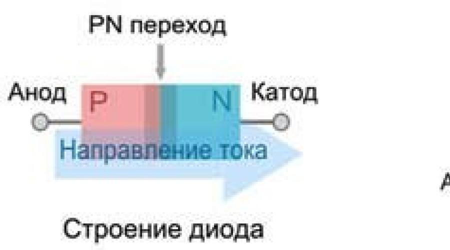
D iodine- the simplest in design in the glorious family of semiconductor devices. If you take a semiconductor plate, for example germanium, and introduce an acceptor impurity into its left half and a donor impurity into the right half, then on one side you will get a semiconductor of type P, respectively, on the other, type N. In the middle of the crystal you will get the so-called P-N junction, as shown in Figure 1.
The same figure shows the conventional graphic designation of a diode in the diagrams: the cathode terminal (negative electrode) is very similar to the “-” sign. It's easier to remember that way.
In total, in such a crystal there are two zones with different conductivities, from which two outputs come out, so the resulting device is called diode, since the prefix “di” means two.
In this case, the diode turned out to be a semiconductor, but similar devices were known before: for example, in the era vacuum tubes there was a tube diode called a kenotron. Now such diodes are a thing of history, although adherents of “tube” sound believe that in tube amplifier even the anode voltage rectifier must be tube-based!

Figure 1. Diode structure and diode designation on the diagram
At the junction of semiconductors with P and N conductivity, it turns out P-N junction, which is the basis of all semiconductor devices. But unlike a diode, which has only one transition, they have two P-N junctions, and, for example, they consist of four junctions at once.
P-N junction at rest
Even if the P-N junction, in this case the diode, is not connected anywhere, interesting physical processes still occur inside it, which are shown in Figure 2.
Figure 2. Diode at rest
In the N region there is an excess of electrons, it carries a negative charge, and in the P region the charge is positive. Together these charges form an electric field. Since unlike charges tend to attract each other, electrons from the N zone penetrate into the positively charged P zone, filling some holes. As a result of such movement, a current, albeit very small (several nanoamperes), appears inside the semiconductor.
As a result of this movement, the density of the substance on the P side increases, but up to a certain limit. Particles usually tend to spread evenly throughout the entire volume of a substance, just as the smell of perfume spreads throughout the entire room (diffusion), so sooner or later the electrons return back to the N zone.
If for most consumers of electricity the direction of the current does not matter - the light bulb lights up, the tile heats up, then for a diode the direction of the current plays a huge role. The main function of a diode is to conduct current in one direction. It is this property that is provided by the P-N junction.
Turning the diode in reverse
If a power source is connected to a semiconductor diode, as shown in Figure 3, then no current will pass through the P-N junction.
Figure 3. Diode reverse connection
As can be seen in the figure, the positive pole of the power source is connected to area N, and the negative pole is connected to area P. As a result, electrons from region N rush to the positive pole of the source. In its turn positive charges(holes) in the P region are attracted by the negative pole of the power supply. Therefore in areas P-N transition, as can be seen in the figure, a void is formed, there is simply nothing to conduct current, there are no charge carriers.
As the voltage of the power supply increases, electrons and holes are attracted more and more strongly electric field batteries, in the region of the P-N junction there are fewer and fewer charge carriers. Therefore, in reverse switching, no current flows through the diode. In such cases it is customary to say that The semiconductor diode is reverse-voltage locked.
An increase in the density of matter near the battery poles leads to occurrence of diffusion, - the desire for a uniform distribution of matter throughout the entire volume. This is what happens when the battery is disconnected.

Semiconductor Diode Reverse Current
This is where the time has come to remember the non-mainstream media that have been conventionally forgotten. The fact is that even in the closed state, a small current passes through the diode, called reverse. This reverse current and is created by minor carriers, which can move in exactly the same way as the main ones, only in the opposite direction. Naturally, such movement occurs under reverse voltage. The reverse current is usually small, which is due to the small number of minority carriers.
As the temperature of the crystal increases, the number of minority carriers increases, which leads to an increase in the reverse current, which can lead to the destruction of the P-N junction. Therefore, operating temperatures for semiconductor devices - diodes, transistors, microcircuits are limited. To prevent overheating, powerful diodes and transistors are installed on heat sinks - radiators.
Turning on the diode in the forward direction
Shown in Figure 4.
Figure 4. Direct connection of the diode
Now let's change the polarity of the source: connect the minus to area N (cathode), and the plus to area P (anode). With this inclusion in the N region, electrons will be repelled from the minus of the battery and move towards side P-N transition. In region P, positively charged holes will be repelled from the positive terminal of the battery. Electrons and holes rush towards each other.
Charged particles with different polarities gather near the P-N junction, and an electric field arises between them. Therefore, the electrons overcome the P-N junction and continue to move through the P zone. In this case, some of them recombine with holes, but most of them rush to the plus of the battery; current Id flows through the diode.
This current is called direct current. It is limited by the technical data of the diode, a certain maximum value. If this value is exceeded, there is a risk of diode failure. It should be noted, however, that the direction of the forward current in the figure coincides with the generally accepted direction, opposite to the movement of electrons.
It can also be said that with the forward direction of switching on, the electrical resistance of the diode is relatively small. When turned on in reverse, this resistance will be many times greater; no current flows through the semiconductor diode (insignificant reverse current is not taken into account here). From all of the above, we can conclude that the diode behaves like an ordinary mechanical valve: turned in one direction - water flows, turned in the other - the flow has stopped. For this property the diode received the name semiconductor gate.
To understand in detail all the abilities and properties of a semiconductor diode, you should get acquainted with its volt-ampere characteristic. It is also a good idea to learn about the different diode designs and frequency properties, advantages and disadvantages. This will be discussed in the next article.
What is forward and reverse voltage? I'm trying to understand the principle of operation of a field-effect transistor. and got the best answer
Answer from Vovik[active]
Direct - a plus is applied to a plus, a minus is applied to a minus. The opposite is true - to a plus - a minus, to a minus - a plus.
Applied to field effect transistor- between source and gate.
There is a base and an emitter bipolar transistor, not at the field.
A bipolar transistor consists of two back-to-back r-n transition and with one common output - emitter - base (common type) - collector, like two diodes, only the common “layer” is thin and conducts current if you apply a direct voltage, which is called opening, between the emitter and the base.
The greater the forward voltage between the base and emitter, the more open the transistor is and the lower its emitter-collector resistance, i.e., there is an inverse relationship between the emitter-base voltage and the resistance of the bipolar transistor.
If a reverse voltage is applied between the base and emitter, the transistor will turn off completely and will not conduct current.
If you apply voltage only to the base and emitter or base and collector, you get a regular diode.
The field-effect transistor is designed somewhat differently. There are also three terminals, but they are called drain, source and gate. There is only one pn junction, gate -> drain-source or gate<- сток-исток в зависимости от полярности транзистора. Затвор находится между истоком и стоком и к нему (измеряется относительно истока) всегда прикладывается только обратное напряжение, которое создаёт поле в промежутке между истоком и стоком, в зависимости от напряжённости больше или меньше препятствующее движению электронов (следовательно, изменяя сопротивление транзистора) , и, таким образом, создающую обратную зависимость между напряжением исток-затвор и сопротивлением полевого транзистора.
Answer from ALEX R[guru]
On the 1st question, direct and reverse direc- tion occurs in a semiconductor (diode), i.e., the diode passes current in the direct direction, but if the current flows in the opposite direction, everything is closed. For clarity, the nipple of a bicycle tire goes there, there is no way back. Field tr-r, just for the sake of understanding, there is no electronic connection between the gate and the drain-source, but the current passes due to the evil field created at the gate. Something like that.
Answer from Alexander Egorov[guru]
direct - minus to the region with n-conductivity, plus to the region k with p-conductivity
the opposite is the opposite
by supplying only the emitter and collector, no current will pass, since the ionized atoms of the base will repel the free charges of the emitter from the pn junction (which are already difficult to jump over the pn junction, since it is a dielectric). And if you apply voltage to the base, it will “suck” free charges from the base and they will no longer repel the emitter charges, preventing them from crossing the pn junction. The transistor will open.
By the way, the emitter, collector and base are not a field-effect transistor, but a bipolar transistor.
If you apply voltage only to the base and emitter or base and collector, then it will be a simple diode (each pn junction is a diode).
Answer from User user[guru]
The field-effect transistor has a p or n type field-controlled channel. transistor terminals gate drain source
Read also:
|
CVC of the diode.
(volt-voltage characteristic) - a graph of the dependence of the current through a two-terminal network on the voltage on this two-terminal network. Most often, the current-voltage characteristic of nonlinear elements is considered (the degree of nonlinearity is determined by the nonlinearity coefficient, since for linear elements the current-voltage characteristic is a straight line and is not of particular interest.
The nonlinearity of the current-voltage characteristic is due to the fact that the resistance of the NE depends on the applied voltage (diodes, zener diodes) or on the current (thermistors). The current-voltage characteristics of nonlinear elements are described by equations whose degrees are higher than the first. Since the resistance of NEs is variable, the instantaneous current value in them is not proportional to the instantaneous voltage values. (p. 117 manual)
Forward and reverse current. Forward and reverse voltage.
When the p-n junction resistance is low, a current called direct current. The larger the area of the p-n junction and the voltage of the power source, the greater this forward current. If the poles of the element are reversed, the diode will be in the closed state. A zone depleted of electrons and holes is formed; it provides very high resistance to the current. However, in this zone a small exchange of current carriers between regions of the diode will still occur. Therefore, a current will flow through the diode, but many times less than the direct current. This current is called reverse diode current. If the diode is connected to a circuit with alternating current, it will open during positive half-cycles at the anode, freely passing current in one direction - forward current Irev., and close during negative half-cycles at the anode, almost without passing current in the opposite direction - reverse current Irev. The voltage at which the diode opens and direct current flows through it is called direct(Upp.), and the voltage of reverse polarity, at which the diode closes and reverse current flows through it, is called reverse(Urev.) At forward voltage, the resistance of a good quality diode does not exceed several tens of ohms, but at reverse voltage its resistance will reach tens, hundreds of kilo-ohms and even mega-ohms.
Breakdown voltage.
A dielectric, being in an electric field, loses its electrical insulating properties if the field strength exceeds a certain critical value. This phenomenon is called dielectric breakdown or violation of its electrical strength. The property of a dielectric to resist breakdown is called electrical strength (Epr). The voltage at which insulation breakdown occurs is called breakdown voltage (Upr).
Published Date: 12/23/2017
Do you know what reverse voltage is?
Reverse voltage

Reverse voltage is a type of energy signal created when the polarity of an electrical current is reversed. This voltage often occurs when reverse polarity is applied to a diode, causing the diode to react by operating in the opposite direction. This reverse function can also create a breakdown voltage within the diode, as this often breaks the circuit to which the voltage is applied.
Reverse voltage occurs when the power signal connection source to a circuit is applied in an inverted manner. This means that the positive lead source is connected to the ground or negative conductor of the circuit and vice versa. This voltage transfer is often not intended, since most electrical circuits are not capable of handling voltages.
When minimum voltage is applied to a circuit or diode, it may cause the circuit or diode to operate in reverse. This may cause a reaction such as the box fan motor turning incorrectly. The element will continue to function in such cases.
When the amount of voltage applied to a circuit is too large, the signal for the receiving circuit, however, is called breakdown voltage. If the input signal that has been reversed exceeds the allowable voltage for the circuit to maintain, the circuit may be damaged beyond the rest of the usable. The point at which the circuit is damaged refers to the breakdown voltage value. This breakdown voltage has a couple of other names, reverse peak voltage or reverse breakdown voltage.
Reverse voltage can cause breakdown voltage, which also affects the operation of other circuit components. Beyond the damaging diodes and reverse voltage circuit functions, it can also become a reverse voltage peak. In such cases, the circuit cannot contain the amount of input power from the signal that has been reversed, and may create a breakdown voltage between the insulators.
This breakdown voltage, which can occur across circuit components, can cause breakdown of components or wire insulators. This can turn them into signal conductors and damage the circuit by conducting voltage to different parts of the circuit that should not receive it, causing instability throughout the circuit. This can cause voltage arcs from component to component, which can also be powerful enough to ignite various circuit components and cause a fire.
Post navigation
Healthy
Renovation interior construction
During the life cycle of a building, renovation work is necessary at certain periods to update the interior. Modernization is also necessary when interior design or functionality lags behind modern times.
Multi-storey construction
There are more than 100 million housing units in Russia, and most of them are “single-family houses” or cottages. In cities, suburbs and rural areas, own homes are a very common type of housing.
The practice of designing, constructing and operating buildings is most often a collective effort among various groups of professionals and professions. Depending on the size, complexity and purpose of a particular building project, the project team may include:
1. The real estate developer who provides financing for the project;
One or more financial institutions or other investors that provide financing;
2. Local planning and management bodies;
3. Service that carries out ALTA/ACSM and construction surveys throughout the project;
4. Building managers who coordinate the efforts of various groups of project participants;
5. Licensed architects and engineers who design buildings and prepare construction documents;
Characteristics and parameters of rectifier and universal diodes
Rectifier diodes are used to rectify low frequency alternating current. The rectifying properties of these diodes are based on the principle of one-way conductivity of electron-hole p-and-junctions.
Universal diodes are used in various electronic equipment as rectifiers alternating current high and low frequencies, multipliers and frequency converters, detectors of large and small signals, etc. The range of operating currents and voltages of rectifier and universal diodes is very wide, so they are produced with both point and planar p-n junctions in the structure of a semiconductor with areas from tenths of a square millimeter to several square centimeters. Typically, universal diodes use junctions with small areas and capacitances, but with relatively high values of forward currents and reverse voltages. These requirements are met by point, microalloy planar and mesaplanar diodes. The characteristics and parameters of universal diodes are the same as those of rectifier diodes.
Volt-ampere characteristics(volt-voltage characteristic) of rectifier diodes expresses the dependence of the current passing through the diode on the value and polarity of the direct voltage applied to it. The direct branch of the characteristic shows the dependence of the current through the diode with the direct through polarity of the applied voltage. The strength of the forward current depends exponentially on the forward voltage applied to the diode and can reach large values with a small (about 0.3 - 1 V) voltage drop across the diode.
The reverse branch of the characteristic corresponds to the non-conducting direction of current through the diode with reverse polarity of the voltage applied to the diode. The reverse current (section OD) slightly depends on the applied reverse voltage. At a relatively high reverse voltage (point B on the characteristic), electrical breakdown of the p-n junction occurs, at which the reverse current quickly increases, which can lead to thermal breakdown and damage to the diode. As the temperature rises, the thermal current and the generation current of charge carriers in the junction will increase, which will lead to an increase in the forward and reverse currents and a shift in the characteristics of the diode.
The properties and interchangeability of diodes are assessed by their parameters. The main parameters include currents and voltages associated with the current-voltage characteristic Diodes are used in both AC and DC circuits. Therefore, to evaluate the properties of diodes, along with the parameters, differential parameters are used that characterize their operation on alternating current.
Rectified (direct) current Ipr is the current (average value per period) passing through the diode, which ensures its reliable and long-term operation. The strength of this current is limited by heating or maximum power Pmax. Exceeding the forward current leads to thermal breakdown and damage to the diode.
- Forward voltage drop UPr.Av - the average value over a period on the diode when the permissible forward current passes through it.
- Allowable reverse voltage U0br is the average value over the period at which reliable and long-term operation of the diode is ensured. Exceeding the reverse voltage leads to breakdown and failure of the diodes. As the temperature increases, the reverse voltage and forward current values decrease.
- Reverse current Irev - average value for the period of reverse current at an acceptable Urev. The lower the reverse current, the better
You are the rectifying properties of the diode. An increase in temperature for every 10 °C leads to an increase in the reverse current for germanium and silicon diodes by 1.5 - 2 times or more.
Maximum constant, or the average power Pmax dissipated by a diode over a period, at which the diode can operate for a long time without changing its parameters. This power is the sum of the products of currents and voltages at the forward and reverse biases of the junction, i.e., for the positive and negative half-cycles of the alternating current. For high-power devices operating with good heat dissipation, Pmax = (Tp.max - Tk)/Rpk. For low power devices operating without a heat sink,
Pmax = (Tp.max - T s) / Rp.s.
Maximum junction temperature Gp.max depends on the material (band gap) of the semiconductor and the degree of its doping, i.e., on the resistivity of the p-n junction region - the base. The Gp.max range for germanium is 80 - 110 °C, and for silicon 150 - 220 °C.
Thermal resistance Rp.k between the transition and the housing is determined by the temperature difference between the junction Tpi housing Tk and the average power Ra released in the transition and is 1 - 3 ° C / W: Ra.K = (Ta - TK) / Pa. The thermal resistance Rn c between the junction and the environment depends on the temperature difference between the junction Tp and the environment Tc. Since practically RPK
The limiting mode of use of diodes is characterized by the maximum permissible reverse voltage URev max, the maximum rectifier current IPr max and the maximum junction temperature TPmax With an increase in the frequency of the alternating voltage supplied to the diode, its rectifying properties deteriorate. Therefore, to determine the properties of rectifier diodes, the operating frequency range Df or the maximum rectification frequency fmax is usually specified. At frequencies greater than fmax, the minority charge carriers accumulated during the forward half-cycle in the base do not have time to compensate, therefore, during the reverse half-cycle of the rectified voltage, the transition remains forward-biased for some time (that is, it loses its rectifying properties). This property is manifested more significantly, the larger the forward current pulse or the higher the frequency of the supplied alternating voltage. In addition, on high frequencies the shunting effect of the barrier and diffusion capacitances of the p-n junction begins to appear, reducing its rectifying properties
When calculating the rectifier mode, the static resistance to direct current and the differential resistance of diodes to alternating current are used
- Differential alternating current resistance rdiff=dU/dI or rDiff=ДU/ДI determines the change in current through the diode when the voltage changes near the selected operating point on the diode characteristic. When the voltage is directly switched on, rdif Pr = 0.026/ /IPr and the current Ipr > 10 mA, it amounts to several ohms. When connecting the reverse voltage, rdif pr is large (from tens of kilo-ohms to several mega-ohms).
- Static diode resistance to direct current rprd = Upr/Ipr, rrev d = Urev/Irev V In the region of forward currents rFor d>rdiff pr, and in the region of reverse currents r0br d
Diode capacitances have a significant impact on their performance at high frequencies and in pulsed modes. The passport data of diodes usually gives the total capacitance of the diode CD, which, in addition to the barrier and diffusion capacitance, includes the capacitance of the device body. This capacitance is measured between the external current leads of the diode at a given reverse bias voltage and current frequency
Semiconductor diode - This is a semiconductor device with one p-n junction and two electrodes. The operating principle of a semiconductor diode is based on the phenomenon p-n junction, so for further study of any semiconductor devices you need to know how it works.
Rectifier diode (also called a valve) is a type of semiconductor diode that serves to convert alternating current to direct current.
The diode has two terminals (electrodes) anode and cathode. The anode is connected to the p layer, the cathode to the n layer. When a plus is applied to the anode and a minus to the anode (direct connection of the diode), the diode passes current. If a minus is applied to the anode and a plus to the cathode (reverse connection of the diode), there will be no current through the diode, this can be seen from the volt-ampere characteristics of the diode. Therefore, when the input of the rectifier diode receives AC voltage Only one half-wave passes through it.

Current-voltage characteristic (volt-ampere characteristic) of the diode.

The current-voltage characteristic of the diode is shown in Fig. I. 2. The first quadrant shows the direct branch of the characteristic, which describes the state of high conductivity of the diode with a forward voltage applied to it, which is linearized by a piecewise linear function
u = U 0 +R D i
where: u is the voltage on the valve when current i passes; U 0 - threshold voltage; R d - dynamic resistance.
In the third quadrant there is a reverse branch of the current-voltage characteristic, which describes the state of low conductivity when a reverse voltage is applied to the diode. In a state of low conductivity, practically no current flows through the semiconductor structure. However, this is only true up to a certain reverse voltage value. With reverse voltage, when the electric field strength in the pn junction reaches about 10 s V/cm, this field can impart to mobile charge carriers - electrons and holes, constantly appearing throughout the entire volume of the semiconductor structure as a result of thermal generation - kinetic energy sufficient for ionization neutral silicon atoms. The resulting holes and conduction electrons, in turn, are accelerated by electrical p-n field transition and also ionize neutral silicon atoms. In this case, an avalanche-like increase in the reverse current occurs, i.e. e. avalanche breakdown.
The voltage at which a sharp increase in reverse current occurs is called breakdown voltage U 3 .
TOPIC 3. SEMICONDUCTOR DIODES
A semiconductor diode is an electrical converter semiconductor device with one electrical junction and two terminals, which uses the properties pn junction A.
Semiconductor diodes are classified:
1) by purpose: rectifier, high-frequency and ultra-high-frequency (HF and microwave diodes), pulse, semiconductor zener diodes (reference diodes), tunnel diodes, reverse diodes, varicaps, etc.;
2) according to design and technological features: planar and point;
3) by type of source material: germanium, silicon, arsenide-gallium, etc.
Figure 3.1 – Design of point diodes
A point diode uses a germanium or silicon plate with n-type electrical conductivity (Fig. 3.1), 0.1...0.6 mm thick and 0.5...1.5 mm2 in area; A sharpened wire (needle) with an impurity deposited on it comes into contact with the plate. In this case, impurities diffuse from the needle into the main semiconductor, which create an area with a different type of electrical conductivity. Thus, a miniature hemispherical pn junction is formed near the needle.
To make germanium point diodes, a tungsten wire coated with indium is welded to a germanium plate. Indium is an acceptor for germanium. The resulting region of p-type germanium is emitter.
Silicon point diodes are made using n-type silicon and a wire coated with aluminum, which serves as an acceptor for the silicon.
In planar diodes, the pn junction is formed by two semiconductors with different types of electrical conductivity, and the junction area is various types diodes range from hundredths of a square millimeter to several tens of square centimeters (power diodes).
Planar diodes are manufactured by fusion (fusing) or diffusion methods (Fig. 3.2).

Figure 3.2 – Design of planar diodes manufactured by alloy (a) and diffusion method (b)
A drop of indium is fused into a plate of n-type germanium at a temperature of about 500°C (Fig. 3.2, a), which, fused with germanium, forms a layer of p-type germanium. The region with p-type electrical conductivity has a higher impurity concentration than the main plate and is therefore an emitter. Lead wires, usually made of nickel, are soldered to the main germanium plate and to the indium plate. If p-type germanium is taken as the starting material, then antimony is smelted into it and then an n-type emitter region is obtained.
The diffusion method of manufacturing a p-n junction is based on the fact that impurity atoms diffuse into the main semiconductor (Fig. 3.2, b). To create a p-layer, the diffusion of an acceptor element (boron or aluminum for silicon, indium for germanium) through the surface of the source material is used.
3.1 Rectifier diodes
A rectifying semiconductor diode is a semiconductor diode designed to convert alternating current into direct current.
Rectifier diodes are made on the basis of a pn junction and have two regions, one of them is lower resistance (contains a higher impurity concentration), and is called the emitter. The other area, the base, is more highly resistant (contains a lower concentration of impurities).
The operation of rectifier diodes is based on the property of one-way conductivity of the p-n junction, which lies in the fact that the latter conducts current well (has low resistance) when connected directly and practically does not conduct current (has a very high resistance) when connected in reverse.
As is known, the forward current of the diode is created by the main ones, and the reverse current is created by non-primary charge carriers. The concentration of majority charge carriers is several orders of magnitude higher than the concentration of non-majority carriers, which determines the valve properties of the diode.
The main parameters of rectifying semiconductor diodes are:
· forward current of the diode Ipr, which is normalized at a certain forward voltage (usually Upr = 1...2V);
· maximum permissible forward current Ipr max diode;
· the maximum permissible reverse voltage of the diode Urev max, at which the diode can still operate normally for a long time;
· constant reverse current Irev flowing through the diode at a reverse voltage equal to Urev max;
average rectified current Ivp.sr, which can pass through the diode for a long time at permissible temperature heating it;
· maximum permissible power Pmax dissipated by the diode, at which the specified reliability of the diode is ensured.
According to the maximum permissible value of the average rectified current, diodes are divided into low-power (Ivp.av £ 0.3A), medium-power (0.3A 10A).
To maintain the performance of a germanium diode, its temperature should not exceed +85°C. Silicon diodes can operate at temperatures up to +150°C.


Figure 3.3 – Change in the volt-ampere characteristics of a semiconductor diode depending on temperature: a – for a germanium diode; b – for a silicon diode
The voltage drop when passing direct current for germanium diodes is DUpr = 0.3...0.6V, for silicon diodes - DUpr = 0.8...1.2V. Large voltage drops when direct current passes through silicon diodes compared to direct voltage drops on germanium diodes are associated with a higher potential barrier height of p-n junctions formed in silicon.
With increasing temperature, the forward voltage drop decreases, which is associated with a decrease in the height of the potential barrier.
When a reverse voltage is applied to a semiconductor diode, a slight reverse current arises in it, due to the movement of minority charge carriers through the pn junction.
As the temperature of the pn junction increases, the number of minority charge carriers increases due to the transition of some electrons from the valence band to the conduction band and the formation of electron-hole charge carrier pairs. Therefore, the reverse current of the diode increases.
When a reverse voltage of several hundred volts is applied to the diode, the external electric field in the blocking layer becomes so strong that it can pull electrons from the valence band into the conduction band (Zener effect). In this case, the reverse current increases sharply, which causes heating of the diode, a further increase in the current and, finally, thermal breakdown (destruction) of the p-n junction. Most diodes can operate reliably at reverse voltages not exceeding (0.7...0.8) Uprob.
The permissible reverse voltage of germanium diodes reaches - 100...400V, and for silicon diodes - 1000...1500V.
In a number of powerful converter installations, the requirements for the average value of the forward current and reverse voltage exceed the nominal value of the parameters of existing diodes. In these cases, the problem is solved by parallel or series connection of diodes.
Parallel connection of diodes is used when it is necessary to obtain a forward current greater than the limiting current of one diode. But if diodes of the same type are simply connected in parallel, then, due to the mismatch of the direct branches of the current-voltage characteristic, they will be differently loaded and, in some, the forward current will be greater than the limiting one.


Figure 3.4 – Parallel connection of rectifier diodes
To equalize currents, diodes with a small difference in the direct branches of the current-voltage characteristic are used (they are selected) or equalizing resistors with a resistance of units of Ohms are connected in series with the diodes. Sometimes additional resistors are included (Fig. 3.4, c) with a resistance several times greater than the direct resistance of the diodes, so that the current in each diode is determined mainly by the resistance Rd, i.e. Rd>>rpr vd. The value of Rd is hundreds of ohms.
Serial connection diodes are used to increase the total permissible reverse voltage. When exposed to reverse voltage, the same reverse current Irev flows through diodes connected in series. however, due to the difference in the reverse branches of the current-voltage characteristic total voltage will be distributed unevenly across the diodes. A diode whose reverse branch of the current-voltage characteristic is higher will have a greater voltage applied to it. It may be higher than the limit, which will lead to breakdown of the diodes.


Figure 3.5 – Series connection of rectifier diodes
To ensure that the reverse voltage is distributed evenly between the diodes regardless of their reverse resistance, diodes are shunted with resistors. The resistances Rsh of the resistors must be the same and significantly less than the smallest reverse resistance of the diodes Rsh 3.2 Zener diodes
A semiconductor zener diode is a semiconductor diode, the voltage on which in the region of electrical breakdown weakly depends on the current and which is used to stabilize the voltage.
Semiconductor zener diodes use the property of a slight change in the reverse voltage at the p-n junction during an electrical (avalanche or tunnel) breakdown. This is due to the fact that a small increase in the voltage at the pn junction in the electrical breakdown mode causes a more intense generation of charge carriers and a significant increase in the reverse current.
Low-voltage zener diodes are made on the basis of heavily alloyed (low-resistance) material. In this case, a narrow planar junction is formed, in which a tunneling electrical breakdown occurs at relatively low reverse voltages (less than 6V). High-voltage zener diodes are made on the basis of lightly alloyed (high-resistance) material. Therefore, their principle of operation is associated with avalanche electrical breakdown.
Main parameters of zener diodes:
· stabilization voltage Ust (Ust = 1…1000V);
· minimum Ist mіn and maximum Ist max stabilization currents (Ist mіn" 1.0...10 mA, Ist max "0.05...2.0A);
· maximum permissible power dissipation Рmax;
· differential resistance in the stabilization section rd = DUst/DIst, (rd" 0.5…200 Ohm);
temperature coefficient of voltage in the stabilization section:

TKU of a zener diode shows by what percentage the stabilizing voltage will change when the temperature of the semiconductor changes by 1°C
(TKU= −0.5…+0.2%/°С).


Figure 3.6 – Volt-ampere characteristic of the zener diode and its symbolic graphic designation
Zener diodes are used to stabilize the voltages of power supplies, as well as to fix voltage levels in various circuits.
Low-voltage voltage stabilization within 0.3...1V can be achieved by using the direct branch of the I-V characteristic of silicon diodes. A diode in which the direct branch of the current-voltage characteristic is used to stabilize the voltage is called a stabistor. There are also double-sided (symmetrical) zener diodes that have a symmetrical current-voltage characteristic relative to the origin.
Zener diodes can be connected in series, with the resulting stabilizing voltage equal to the sum of the zener diode voltages:
Ust = Ust1 + Ust2 +…
Parallel connection of zener diodes is unacceptable, because due to the scatter of characteristics and parameters of all parallel-connected zener diodes, current will arise only in one, which has the lowest stabilizing voltage Ust, which will cause overheating of the zener diode.
3.3 Tunnel and reverse diodes
A tunnel diode is a semiconductor diode based on a degenerate semiconductor, in which the tunnel effect leads to the appearance of a negative differential resistance section on the current-voltage characteristic at forward voltage.
The tunnel diode is made of germanium or gallium arsenide with a very high concentration of impurities, i.e. with very low resistivity. Such semiconductors with low resistance are called degenerate. This makes it possible to obtain a very narrow pn junction. In such transitions, conditions arise for relatively free tunneling of electrons through a potential barrier (tunnel effect). The tunnel effect leads to the appearance of a section with negative differential resistance on the direct branch of the diode’s current-voltage characteristic. The tunnel effect is that at a sufficiently low height of the potential barrier, electrons can penetrate through the barrier without changing their energy.
Main parameters of tunnel diodes:
· peak current Iп – forward current at the maximum point of the current-voltage characteristic;
· valley current Iв – forward current at the minimum point of the current-voltage characteristic;
· ratio of tunnel diode currents Iп/Iв;
· peak voltage Uп – forward voltage corresponding to the peak current;
· valley voltage Uв – forward voltage corresponding to the valley current;
· solution voltage Uрр.
Tunnel diodes are used to generate and amplify electromagnetic oscillations, as well as in high-speed switching and pulse circuits.

Figure 3.7 – Current-voltage characteristic of a tunnel diode
A reverse diode is a diode based on a semiconductor with a critical concentration of impurities, in which the conductivity at reverse voltage due to the tunneling effect is significantly greater than at forward voltage.
The principle of operation of a reverse diode is based on the use of the tunnel effect. But in reverse diodes the concentration of impurities is lower than in conventional tunnel diodes. Therefore, the contact potential difference for reversed diodes is smaller, and the thickness of the pn junction is greater. This leads to the fact that under the influence of direct voltage, a direct tunnel current is not created. The forward current in reversed diodes is created by the injection of non-majority charge carriers through the p-n junction, i.e. direct current is diffusion. When the voltage is reversed, a significant tunneling current flows through the junction, created by the movement of electrons through the potential barrier from the p-region to the n-region. The working section of the current-voltage characteristic of a reversed diode is the reverse branch.
Thus, reversed diodes have a rectifying effect, but their passing (conducting) direction corresponds to reverse connection, and the blocking (non-conducting) direction corresponds to direct connection.

Figure 3.8 – Volt-ampere characteristic of a reversed diode
Reversed diodes are used in pulsed devices, and also as signal converters (mixers and detectors) in radio engineering devices.
3.4 Varicaps
A varicap is a semiconductor diode that uses the dependence of capacitance on the magnitude of the reverse voltage and is intended for use as an element with electrically controlled capacitance.
The semiconductor material for the manufacture of varicaps is silicon.
Basic parameters of varicaps:
· nominal capacitance Sv – capacitance at a given reverse voltage (Sv = 10...500 pF);
Capacity overlap coefficient; (Ks = 5...20) – the ratio of the varicap capacitances at two given values of reverse voltages.
Varicaps are widely used in various circuits for automatic frequency adjustment and in parametric amplifiers.

Figure 3.9 – Capacitance-voltage characteristic of a varicap
3.5 Calculation electrical circuits with semiconductor diodes.
In practical circuits, some load, for example a resistor, is connected to the diode circuit (Fig. 3.10, a). Direct current flows when the anode has a positive potential relative to the cathode.
The mode of the diode with a load is called the operating mode. If the diode had linear resistance, then calculating the current in such a circuit would not be difficult, since the total resistance of the circuit is equal to the sum of the diode's resistance to direct current Ro and the resistance of the load resistor Rн. But the diode has a nonlinear resistance, and its Ro value changes as the current changes. Therefore, the current calculation is done graphically. The task is as follows: the values of E, Rn and the characteristics of the diode are known; it is required to determine the current in the circuit I and the voltage on the diode Ud.

Figure 3.10
The diode characteristic should be considered as a graph of some equation connecting the quantities I and U. And for resistance Rн, a similar equation is Ohm’s law:
 (3.1)
(3.1)
So, there are two equations with two unknowns I and U, and one of the equations is given graphically. To solve such a system of equations, you need to construct a graph of the second equation and find the coordinates of the point of intersection of the two graphs.
The equation for resistance Rн is an equation of the first degree with respect to I and U. Its graph is a straight line called the load line. It is constructed using two points on the coordinate axes. For I= 0, from equation (3.1) we obtain: E − U= 0 or U= E, which corresponds to point A in Fig. 3.10, b. And if U= 0, then I= E/Rн. we plot this current on the ordinate axis (point B). We draw a straight line through points A and B, which is the load line. The coordinates of point D give the solution to the problem.
It should be noted that a graphical calculation of the diode operating mode can be omitted if Rн >> Ro. In this case, it is permissible to neglect the resistance of the diode and determine the current approximately: I»E/Rн.
The considered method for calculating direct voltage can be applied to amplitude or instantaneous values if the source provides alternating voltage.
Since semiconductor diodes conduct current well in the forward direction and poorly in the reverse direction, most semiconductor diodes used for rectifying alternating current.
The simplest circuit for rectifying alternating current is shown in Fig. 3.11. It is connected in series with a source of alternating EMF - e, a diode VD and a load resistor Rн. This circuit is called half-wave.
The simplest rectifier works as follows. During one half-cycle, the voltage for the diode is direct and a current passes, creating a voltage drop UR across the resistor Rн. During the next half-cycle, the voltage is reversed, there is practically no current and UR = 0. Thus, a pulsating current passes through the diode and load resistor in the form of pulses lasting half a cycle. This current is called rectified current. It creates a rectified voltage across the resistor Rн. Graphs in Fig. 3.11, b illustrate the processes in the rectifier.

Figure 3.11
The amplitude of the positive half-waves on the diode is very small. This is explained by the fact that when direct current passes, most of the source voltage drops across the load resistor Rн, the resistance of which significantly exceeds the resistance of the diode. In this case
For conventional semiconductor diodes, the forward voltage is no more than 1...2V. For example, let the source have an effective voltage E = 200V and ![]() . If Up max = 2V, then URmax = 278V.
. If Up max = 2V, then URmax = 278V.
With a negative half-wave of the supplied voltage, there is practically no current and the voltage drop across the resistor Rн is zero. The entire source voltage is applied to the diode and is the reverse voltage for it. Thus, the maximum value of the reverse voltage is equal to the amplitude of the source emf.
The simplest diagram of using a zener diode is shown in Fig. 3.12, a. The load (consumer) is connected in parallel with the zener diode. Therefore, in stabilization mode, when the voltage on the zener diode is almost constant, the same voltage will be on the load. Usually Rogr is calculated for the midpoint T of the zener diode characteristics.
Let's consider the case when E = const, and Rн varies from Rн min to Rн max..
The value of Rolim can be found using the following formula:
 (3.3)
(3.3)
where Iav = 0.5(Ist min+Ist max) – average zener diode current;
Iн = Ust/Rн – load current (at Rн = const);
In.av = 0.5(In min+In max), (with Rn = var),
and  And
And  .
.

Figure 3.12
The operation of the circuit in this mode can be explained as follows. Since Rogr is constant and the voltage drop across it, equal to (E − Ust), is also constant, then the current in Rogr, equal to (Ist + In.sr), must be constant. But the latter is only possible if the zener diode current I and the load current Iн change to the same extent, but in opposite directions. For example, if In increases, then the current I decreases by the same amount, and their sum remains unchanged.
Let's consider the principle of operation of a zener diode using the example of a circuit consisting of a series-connected source of variable EMF - e, a zener diode VD and a resistor R (Fig. 3.13, a).
During the positive half-cycle, a reverse voltage is applied to the zener diode, and up to the breakdown voltage of the zener diode, all voltage is applied to the zener diode, since the current in the circuit is zero. After electrical breakdown of the zener diode, the voltage on the zener diode VD remains unchanged and the entire remaining voltage of the EMF source will be applied to resistor R. During the negative half-cycle, the zener diode is switched on in the conducting direction, the voltage drop across it is about 1V, and the remaining voltage of the EMF source is applied to resistor R.
A semiconductor diode is a semiconductor device with one electrical junction and two terminals, which uses one or another property of the electrical junction. The electrical junction can be an electron-hole junction, a metal-semiconductor junction, or a heterojunction.
The region of the diode semiconductor crystal that has a higher concentration of impurities (and therefore the majority charge carriers) is called the emitter, and the other, with a lower concentration, is called the base. The side of the diode to which the negative pole of the power source is connected when connected directly is often called the cathode, and the other is called the anode.
According to their purpose, diodes are divided into:
1. rectifiers (power), designed to convert alternating voltage from industrial frequency power supplies to direct voltage;
2. Zener diodes (reference diodes) designed to stabilize voltages , having on the reverse branch of the current-voltage characteristic a section with a weak dependence of voltage on the flowing current:
3. varicaps intended for use as a capacitance controlled by electrical voltage;
4. pulse, designed to work in high-speed pulse circuits;
5. tunnel and reverse, designed to amplify, generate and switch high-frequency oscillations;
6. ultra-high-frequency, designed for conversion, switching, and generation of ultra-high-frequency oscillations;
7. LEDs designed to convert an electrical signal into light energy;
8. photodiodes, designed to convert light energy into an electrical signal.
The system and list of parameters included in the technical descriptions and characterizing the properties of semiconductor diodes are selected taking into account their physical and technological features and scope of application. In most cases, information about their static, dynamic and limit parameters is important.
Static parameters characterize the behavior of devices when DC, dynamic - their time-frequency properties, limiting parameters determine the area of stable and reliable operation.
1.5. Current-voltage characteristic of the diode
The current-voltage characteristic (volt-ampere characteristic) of the diode is similar to the current-voltage characteristic p-n-transition and has two branches – forward and reverse.
The diode's current-voltage characteristic is shown in Figure 5.
If the diode is turned on in the forward direction ("+" - to the area R, and “-” – to the area n), then when the threshold voltage is reached U Then the diode opens and direct current flows through it. When turned back on ("-" to the area R, and “+” – to the area n) an insignificant reverse current flows through the diode, that is, the diode is actually closed. Therefore, we can consider that the diode passes current in only one direction, which allows it to be used as a rectifier element.
The values of the forward and reverse currents differ by several orders of magnitude, and the forward voltage drop does not exceed a few volts compared to the reverse voltage, which can be hundreds or more volts. The rectifying properties of diodes are better, the lower the reverse current at a given reverse voltage and the lower the voltage drop at a given forward current.
The parameters of the current-voltage characteristic are: dynamic (differential) resistance of the diode to alternating current and static resistance to direct current.
The static resistance of the diode to direct current in the forward and reverse directions is expressed by the relation:
 , (2)
, (2)
Where U And I specify specific points on the diode’s current-voltage characteristic at which the resistance is calculated.
Dynamic AC resistance determines the change in current through a diode with a change in voltage near a selected operating point on the diode characteristic:
 . (3)
. (3)
Since a typical I-V characteristic of a diode has sections with increased linearity (one on the forward branch, one on the reverse branch), r d is calculated as the ratio of a small voltage increment across the diode to a small current increment through it at a given mode:
 . (4)
. (4)
To derive an expression for r d, it is more convenient to take current as an argument I, and consider the voltage as a function and, taking the logarithm of equation (1), bring it to the form:
 . (5)
. (5)
 . (6)
. (6)
It follows that with increasing forward current r d decreases quickly, since when the diode is turned on directly I>>I S .
In the linear section of the current-voltage characteristic when the diode is connected directly, the static resistance is always greater than the dynamic resistance: R st > r d. When turning the diode back on R st r d.
Thus, the diode's electrical resistance in the forward direction is much less than in the reverse direction. Therefore, the diode has one-way conductivity and is used to rectify alternating current.