Instructions for using jtag programmer. AVR in-circuit debugging via JTAG ICE
Any person more or less interested in electronics today knows what “firmware” is. Many people in this category encountered the “firmware crash” situation. The most unpleasant subtype of the situation is the “brick” state. Below the cut is a little theory and practice of “spraying” using the hero device of the review.
I do not professionally repair electronics and am not trying to make money from it. But the research itch, coupled with minimal knowledge in the field of electronics and computer science, sometimes pushes me to get into the guts of some next device (and, as a result, unplanned purchases).
Background.
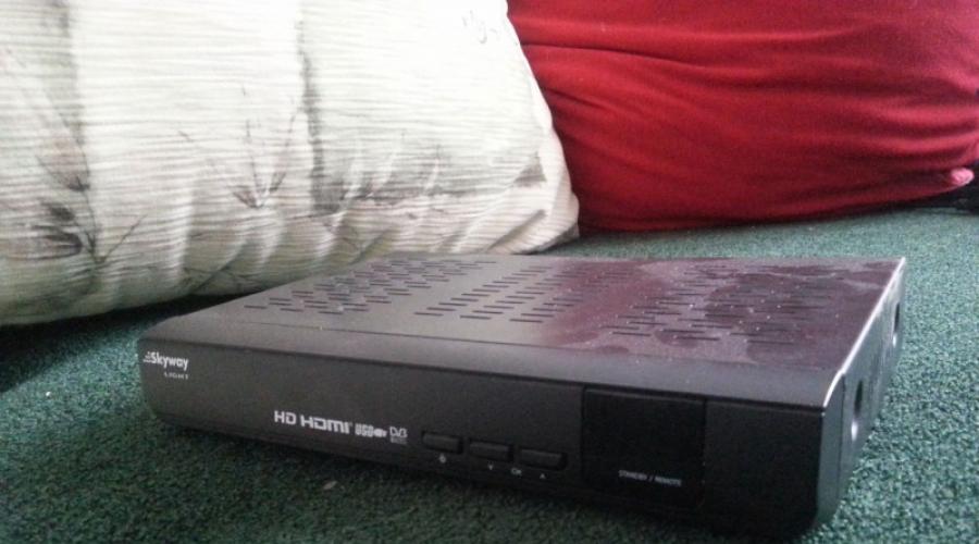
Once, while visiting a friend, I came across a satellite tuner lying in a pile of rubbish, still quite modern.

It turned out that the device was faulty with the following symptoms: it once loaded on the second try, then it started booting on the third, then on the fifth, then on the tenth, then it stopped completely. The service center charged an inadequate amount for repairs; as a result, a new tuner was simply purchased, and this one was thrown into a pile of rubbish. The owner happily agreed to the offer to buy it for a symbolic sum, as a result I became the owner of a faulty Skyway Light tuner with an almost complete set - I found a remote control, a power supply and even a remote IR receiver.
First start.
Oddly enough, it turned on for me not the twentieth time, but only the third. I scanned the channels and started showing. But when I tried to launch the Youtube application it froze. The next ten reboots using the power switch method did not lead to anything. The previous owner did not deceive me.
First suspicion. Nutrition.
The Internet is full of reports on reviving tuners by restoring supply voltages. Usually it is enough to replace swollen electrolytic capacitors in the “cold” part of the power supply. But this clearly promised not to be my case. Firstly, the power supply is remote, replacing it with a similar one from a working tuner did not help. Secondly, there were no large electrolytic capacitors on the board, mostly small signal capacitors in analog circuits.
Second suspicion. Firmware.
It was not possible to update the firmware either from the flash drive by pressing the down button, or through the COM port using the Porter Express program. In the first case, the read indicator on the flash drive blinked for several seconds, after which there was silence. In the second, the program displayed a “recording error” message without any explanation, which did not suit it. This is how I came to the third suspicion.
The third suspicion. Flash memory chip.
Several facts prompted this idea. Firstly, in the download console, which became available after connecting via the COM port, the message “CRC error” appeared at startup. Secondly, when trying to remove the tuner configuration using Porter Express, the merged file turned out different each time, not matching the previous one during a byte-by-byte comparison.
A quick study of Aliexpress showed that such a chip can be purchased for little money. But here the main problem emerged: just buying a flash drive is not enough. It needs to be flashed. Either on the programmer or directly on the board. In my case, this is the Spansion S29GL256P90TFCR2 chip - parallel flash memory in a TSOP-56 package. The search for such a programmer, either among electronics friends or in online stores at an adequate price, was not successful. The only option left is to flash the flash drive directly on the board after soldering. And here, for the first time, a phrase was mentally uttered, which usually sounds like a sentence on electronics forums: “only JTAG will help.”
A little about JTAG.
Almost every modern system-on-chip has the ability to debug and test. Most often it is implemented as a serial interface with input, output, clock, select and reset signals, which is called JTAG. Typically, these pins are routed on the board in the form of pins or pads. The problem is that only the electrical interface is standardized. The commands for controlling a specific chip are individual; moreover, most manufacturers do not disclose them and they have to be figured out using reverse engineering. That is why there are practically no tools in the public domain for working with modern popular chipsets.
Order an adapter.
Googling commercial products that can work with my ST40 chipset led me to the ejtag.ru resource, where there is a repair community and a small online store. Having looked for the cheapest adapter and made sure that it can work with ST40, I began negotiations with Toad and began the purchasing process. The process is different from what we are used to in popular online stores. No PayPal or disputes. We register, add the item to the cart, and place an order. After some time, a message arrives with the WM wallet number and the amount to pay. We pay, confirmation of payment arrives, and a few days later - notification of shipment. All that remains is to wait. The guarantee of the transaction is the good name of the seller.
Receipt, unpacking, registration.
A plastic bag of Russian post, inside wrapped in bubble wrap and placed in an antistatic bag, an adapter, a USB A male - Mini USB cable, a cable with a ten-pin block (will be visible in other photos, at the time of shooting it was hooked up to the tuner), an adapter for flashing serial flash drives of the most popular ones series - 25th, 93rd and in theory 24th.


To estimate sizes

Photos of the insides
Inside is a microcontroller with an 8051 command system and a buffer chip.


The screenshot shows the entire purchase process, including the request for a registration code after receipt:

Order a new flash drive on Aliexpress.
I won’t describe it in detail. I ordered it, it took almost two months, it came in a plastic blister, which was in a standard package.

I ordered 2 pieces, in case I killed one when resoldering.

Resoldering a flash drive.
Soldering small chips has been described many times on Youtube. The key to success here is the presence of a soldering station with a hair dryer, good flux, and straight hands. In short: we blow off the old chip, tin the pads with low-melting solder, apply flux, blow with a hairdryer (with the correct air flow and temperature) until the chip is seated, go over the top with a regular soldering iron for reliability.


The photo shows that it didn't turn out very well. The legs moved a little, and the sight of unwashed flux may cause some repairmen to press their hand to their face. But for personal use it will do.
Firmware.
The JTAG pinout for my tuner is on the store forum. We solder to the contact pads on the board.

Everything is ready for firmware.

Let's launch the program.

Select the processor type from the list. Click the “Connect” button.

A bunch of service information runs through the list; the “Read” and “Write” and “Erase” buttons become active. Usually it is recommended to flash only the bootloader, and then flash it through it in the usual way from a USB flash drive. But I uploaded a full dump, 32 megabytes - I was too lazy to bother with unpacking a separate bootloader. The firmware took about half an hour, the result is in the photo:

Resume.
When developing and debugging programs for microcontrollers, questions arise related to programming and debugging the program in a real circuit. If there are no special problems with programming AVR microcontrollers, since there are many circuits for “pouring” firmware into a crystal, one of the simplest such circuits is a circuit called “five wires”, then there is no such rich choice when debugging a program.
To debug a program, it is possible to use only two options - a software simulator and an in-circuit JTAG emulator-programmer. A software simulator, as a rule, cannot take into account all the operating features of the circuit, such as external influences, joint operation with other devices, etc. With hardware JTAG programmer-debuggers, it becomes possible to step-by-step debug a program directly in the microcontroller itself installed directly into the circuit, view and change all registers of the microcontroller, set breakpoints and, of course, in-circuit programming of the microcontroller. But the cost of the original AVR JTAG ICE MkII produced by Atmel fluctuates around 300 euros, and its analogue AVDRAGON mass-produced, it costs about 3,000 rubles, which is very expensive for people who create devices on AVR microcontrollers “for themselves.”
But fortunately we managed to create a clone of the original AVR JTAG ICE, which costs significantly less than the original and allows programming and debugging of AVR microcontrollers with a JTAG interface.
Fig 1. Circuit diagram of the AVR JTAG ICE clone
The electrical circuit diagram is shown in Fig. 1. The basis of this JTAG is the DD3 AVR ATMega16 microcontroller. The DD2 MAX232 chip acts as a converter of the RS232 interface to TTL UART levels. The DD1 chip is designed to protect the input and output circuits of the DD3 microcontroller and match the voltage of logic levels when using external power.
JTAG power can be taken from the power circuits of the device being debugged through the fourth pin vTref XP3, and can also be used externally through the XP1 and XP2 connectors. External voltage can be in the range from 7 to 15V. When using an external power source, the vTref pin of the XP3 connector does not need to be connected.
LED HL2 displays the presence of power, HL1 is the JTAG operating mode.
JTAG is connected to the microcontroller being debugged via a standard ten-pin connector. The connection diagram of which is shown in Fig. 2.

Fig 2. Connection diagram of AVR JTAG ICE to the device being debugged
There are several options for BootLoader bootloaders for JTAG firmware, but in my opinion, the most successful option was made by Vitaly Krotevich (Vit). Its bootloader most closely replicates the proprietary one and allows you to update the JTAG firmware directly from AVRStudio without rebooting the JTAG and entering programming mode via BootStart. If you do not plan to update the JTAG firmware, then you can not flash the bootloader, but only “flash” the original firmware from .
To “hardwire” the bootloader into JTAG, you can use the AVReal, PonyProg, STK200, “five wires” programmer, or any other available and compatible with AVR ISP. The programmer is connected to the ISP programming connector XP4. Firmware file JTAG_ICE.hex.
An example of fuse programming is shown in Figure 3.

Fig 3. Setting fuses for AVR JTAG ICE
An example of AVR JTAG ICE operation is shown in Figure 4. As an example, the ATMega128 signature was read

Figure 4. Reading the ATMega128 microcontroller signature using AVR JTAG ICE

Fig 5. Image of the top layer of the PCB trace, with applied elements

Fig 6. Image of the bottom layer of the PCB trace, with applied elements
Photos of the finished device:


P.S. The circuit diagram and trace of the printed circuit board were developed by the author of the article, the bootloader was used by Vitaliy Krotevich (aka Vit), the firmware was from the original AVRStudio.
The following sources were used when writing this article:
1 http://onembedding.bialix.com/files/jtag_vit/
2. Official AVR JTAG ICE User Guide JTAGuserguide.pdf
You can download the firmware and PCB files below
List of radioelements
| Designation | Type | Denomination | Quantity | Note | Shop | My notepad |
|---|---|---|---|---|---|---|
| DD1 | Buffer IC, driver | CD74AC244 | 1 | To notepad | ||
| DD2 | RS-232 interface IC | MAX232 | 1 | ST232BD | To notepad | |
| DD3 | MK AVR 8-bit | ATmega16 | 1 | ATmega16-16PI | To notepad | |
| DA1 | Linear regulator | LM78L05 | 1 | To notepad | ||
| VD1, VD2 | Rectifier diode | SM4007PL | 2 | To notepad | ||
| VD3 | Zener diode | BZX55C5V1 | 1 | SMBJ5.0A | To notepad | |
| VD4, VD5 | Schottky diode | SM5819PL | 2 | To notepad | ||
| HL1, HL2 | LED | KR-3216-2 | 2 | To notepad | ||
| C1, C2, C4-C6, C9-C13, C16 | Capacitor | 0.1 µF | 10 | To notepad | ||
| C3 | 1 | To notepad | ||||
| C7 | Electrolytic capacitor | 470 µF 10 V | 1 | Tantalum | To notepad | |
| C8 | Capacitor | 1200 pF | 1 | To notepad | ||
| C14, C15 | Capacitor | 22 pF | 2 | To notepad | ||
| R1 | Resistor | 36 kOhm | 1 | To notepad | ||
| R2 | Resistor | 150 kOhm | 1 | To notepad | ||
| R3-R6 | Resistor | 10 kOhm | 4 | To notepad | ||
| R4, R10 | Resistor | 4.7 kOhm | 2 | To notepad | ||
| R9, R11-R15 | Resistor | 200 Ohm | 7 | To notepad | ||
| R16 | Resistor |
There are many microcontroller programmer circuits available on the Internet. I present a version of an in-circuit universal USB programmer with debugging capabilities, which I use. You can assemble this programmer with your own hands.
The basis of the programmer is the FT2232D chip. It is a USB to two UART ports converter. The peculiarity is that the “upper” channel A can operate in JTAG, SPI and I 2 C modes, which is required for programming microcontrollers, various memory chips, etc.
The development of this USB programmer is carried out on a computer using libraries from FTDI Chip.
The device is powered from the USB interface. If assembled correctly, the circuit does not need to be configured. The functioning of the device depends on the skill of the software developer. Resistors R8, R9, R12, R13, R14, R15, R16 are current-limiting if connected incorrectly to the device; accordingly, the terminals of the programmable device should not be connected to other elements in the circuit, or have such pull-ups that would not distort the logical logic when forming voltage dividers levels. Chip U1 is used to save user settings.
U2 pins (channel A):
24 - ADBUS0 – output - in JTAG TCK mode, in SPI SK mode;
23 - ADBUS1 – output - in JTAG TDI mode, in SPI DO mode;
22 - ADBUS2 – input - in JTAG TDO mode, in SPI DI mode;
21 - ADBUS3 – output - in JTAG TMS mode, in SPI mode as an auxiliary signal (CS);
20 - ADBUS4 – in JTAG mode input/output, in SPI mode auxiliary output. This pin is used to provide a RESET signal to the microcontroller;
15 - AСBUS0 – freely programmable input/output in all modes (optionally used to supply power to the programmable device);
13 - AСBUS1 – freely programmable input/output in all modes.
In principle, these conclusions are multifunctional. Their behavior is determined by the selected mode when the port is opened.
Channel B is used to debug the programmable device. To do this, you only need to have an unused UART port in the microcontroller. Next is a matter of technology. In the microcontroller program, we use the formatted output function printf() in the right places.
40 -BDBUS0 – output - in UART TXD mode;
39 -BDBUS1 – input - in UART RXD mode;
28 - BСBUS2 – output - in UART mode LED indicator (lights up when transmitting data via USB);
27 - BСBUS3 – output - LED indicator in UART mode (lights up when receiving data via USB).
Below is the programmer circuit board


Today, this universal programmer supports AVR microcontrollers via JTAG and SPI interfaces. Moreover, the speed of Atmega64 firmware via JTAG is no more than 5 seconds, via SPI no more than 8 seconds. In principle, you can flash any microcontrollers to which the specification for the programmer applies. Currently, for example, development is underway to support NEC microcontrollers.

The working form is divided into two parts: on the left are tables for working with FLASH (top) and EEPROM (bottom), here you can open files or download firmware from the microcontroller, do verification, edit the contents of memory cells; on the right is a text field for debugging, data from channel B is displayed here, you can also enter text there that will be sent to the port (functionally this is an analogue of HyperTerminal). Development is carried out on the Visual C# platform for Windows. It is also possible to develop in other languages. The programmer can also work under Linux.

Literature used:
1. A.V. Evstigneev “AVR microcontrollers of the Tiny and Mega families from ATMEL”, M. Publishing house “Dodeka-XXI”, 2005.
2. Future Technology Devices International Ltd. “FT2232D Dual USB UART/FIFO I.C.” ,Datasheet, 2006.
3. Future Technology Devices International Ltd. “Software Application Development D2XX Programmer's Guide”, Document, 2009.
4. Future Technology Devices International Ltd. “Programmers Guide for High Speed FTCJTAG DLL”, Application note AN_110, 2009.
5. Future Technology Devices International Ltd. “Programmers Guide for High Speed FTCSPI DLL”, Application note AN_111, 2009.
6. Andrew Troelsen “C# and the .NET platform” M., S-P. Peter, 2007.
You can download the software sources and printed circuit board in the format below
Borisov Alexey () Syzran, Samara region.
List of radioelements
| Designation | Type | Denomination | Quantity | Note | Shop | My notepad |
|---|---|---|---|---|---|---|
| U1 | Chip | AT93C46D-8S | 1 | To notepad | ||
| U2 | Chip | FT2232D | 1 | To notepad | ||
| VT1 | MOSFET transistor | BSS84 | 1 | To notepad | ||
| C1 | Capacitor | 0.01 µF | 1 | To notepad | ||
| C2, C3 | Capacitor | 27 pF | 2 | To notepad | ||
| C4, C5, C7, C9, C10 | Capacitor | 0.1 µF | 5 | To notepad | ||
| C6 | Capacitor | 0.033 µF | 1 | To notepad | ||
| C8 | Electrolytic capacitor | 10 µF | 1 | To notepad | ||
| R1 | Resistor | 2.2 kOhm | 1 | 0.05W | To notepad | |
| R2 | Resistor | 10 kOhm | 1 | 0.05W | To notepad | |
| R3, R4 | Resistor | 27 Ohm | 2 | 0.05W | To notepad | |
| R5 | Resistor | 470 Ohm | 1 | 0.05W | To notepad | |
| R6, R7 | Resistor | 1.5 kOhm | 2 | 0.05W | To notepad | |
| R8-R16 | Resistor |
I found a photo in my archive that showed the manufacturing process of the JTAG programmer that I needed to revive the satellite tuner. Now a little more detail about what kind of “beast” JTAG is:
JTAG(short for English) Joint Test Action Group; pronounced “jay-tag”) is the name of the working group for the development of the IEEE 1149 standard. Later, this abbreviation became firmly associated with the specialized hardware interface developed by this group based on the IEEE 1149.1 standard. Official name of the standard Standard Test Access Port and Boundary-Scan Architecture. The interface is designed to connect complex digital circuits or PCB-level devices to standard test and debugging equipment. For those interested, see the full article at Wikipedia.
Now let’s get back to business, my friends gave me a satellite tuner, the most common and simple Globo on an Ali M3329B processor. With such symptoms, it didn’t turn on at all, at first I blamed the power supply, but after checking all the voltages with a multimeter, it turned out that everything was fine with the power supply. After studying a few different articles on repairing these receivers, I came to the conclusion that judging by the symptoms, the firmware was completely lost, and it can be restored by flashing it through a JTAG programmer. There was also the thought that it was completely burned out and could not be restored, but I still preferred to believe that firmware via JTAG would help.
For production I chose this scheme:

Power is supplied to the circuit from the receiver to which it is connected. There is no need to use an external power supply for the circuit for two reasons. Firstly, the current consumption is very small and does not create additional load on the receiver’s power supply, and secondly, power supply from the same source as the processor with flash memory improves the matching of logical levels.
The 74HC244 is not an inverting buffer. The chip contains two independent four-bit buffers. Each buffer has its own output enable signal (active low). There are no Schmitt triggers at the inputs. The microcircuit is made using “fast” CMOS technology, which ensures high performance. The powerful current output makes it possible to maintain high performance even with a capacitive load. The performance of the 74HC244 is comparable to that of chips based on Schottky diodes, while the 74HC244 retains the advantages of CMOS chips, i.e. high noise immunity and low power consumption. The inputs of the microcircuit are protected from damage by static electricity using diodes.
Alas, I did not find the 74HC244 in my supplies. I found only an analogue of 74F244, which differed slightly in the supply voltage Vcc. The 74HC244 has a recommended voltage of 2 to 6 V, and the 74F244 has a recommended voltage of 4.5 to 5.5 V. Although the maximum limits are from -0.5 to +7 V, so I decided not to bother and start manufacturing.
Taking the original diagram in the first image and redrawing it in the DipTrace program, we got this diagram:


Everything was traced automatically, only one line was not traced, but this problem was solved by two SMD jumpers. The image above is a printed circuit board ready for manufacturing.
On the board I also signed all the pins, but unfortunately I signed the output signals incorrectly, as can be seen on the original source 1- GND, 2- TCK, 3- TMS, 4- TDO, 5- TDI and 6- RST, but I got it GND, TMS, TCK, TDI, TDO, and RST, I made a mistake when I signed the contacts, according to the diagram everything is correct, according to the original source, i.e. 1- GND, 2- TCK, 3- TMS, 4- TDO, 5- TDI and 6- RST.
PCB with correct pin designations:


Actually, the main thing is a getinax, a file, a small hand saw, sandpaper. A screwdriver and a cutter for splitting the getinax into 2 parts, since my piece was foil-coated on both sides, and our board is simple, one-sided.
Having done all the work, turning the getinax to the size of the board (approximately 55x50 mm), we take the COMET cleaning agent in powder and a dishwashing sponge. We clean the getinax from traces of fat and dirt. It is better not to wipe off the remaining water, but to let it dry.
While the getinax is drying, we go to the computer and print our diagram on a laser printer and photo paper in mirror image, indicating the maximum print quality. It is important not to forget to set the mirror image, otherwise we will end up with everything on the board inside out!
And so, the getinax is ready, the printed circuit board is printed, carefully fitting the edges of the getinax to the design of the printed circuit board on photo paper, attach it to the getinax with adhesive paper tape, take the iron and set it to the maximum temperature.

Naturally, the foil side of the getinaks to the printed circuit board pattern.
When the iron has warmed up, pressing tightly, we begin to iron - evenly heating the getinaks from the paper side. We heat a board of this size for no more than 30-60 seconds, otherwise the toner will spread. I recommend setting a timer on your phone so that the time is close to you, before your eyes. When everything is done, let the board cool down.
We tear off the photo paper from the board, in front of us is a finished board, which remains to be etched in ferric chloride FeCl₃, if there are minor flaws, before etching, we correct the tracks with a scalpel and a thin marker for disks.

During the etching process with ferric chloride, it is necessary to continuously stir the solution, for example by shaking the glassware. If the size of the board is not very large, you can place the board on the surface of the solution with the pattern down - there is no need to shake it, but it is difficult to track the end of the etching process. The etching time with ferric chloride ranges from 5 to 50 minutes and depends on the temperature, concentration of the solution and its contamination with copper, and the thickness of the copper foil. After etching, the board must be rinsed with running water and dried.
As a result, we get this printed circuit board

We also clean the toner with Comet powder, it holds up quite well, and so as not to damage the board tracks, we clean it slowly.
After cleaning the toner we see a neat, beautiful printed circuit board


Now let's start soldering the elements:

- An official programmer produced by Atmel costs approximately 300 euros(without delivery and customs clearance). A cheaper option - you can find unofficial “clones” for about $150 .
- The option is even cheaper, but requires effort, because... from the "do it yourself" category:
on the web through a search engine ( clone AVR-JTAGICE mkII) you can easily find a diagram with the programmer firmware accompanied by assembly instructions.
Programmer characteristics
- Full support for JTAG programming, also supports ISP and DebugWire interfaces.
- Connection to PC is carried out using USB 1.1 or RS-232 interface
- Breakpoints at program memory and data memory addresses
- All operations and breakpoints are executed in real time
- The voltage supplied to the circuit being debugged is 1.8-5.5 V
- The external power supply voltage is 9-12V, the debugger can also be powered from a USB port
Programmer AVR-JTAGICE3
Official programmer for Atmel microcontrollers of the AVR family that support the JTAG debugging and programming interface.
I think for debugging AVR microcontrollers in the AVR Studio 5 environment is the best choice. By the way, I couldn’t find any unofficial clones. If anyone knows, please let me know in the comments to the page.
When I started using it, I experienced some difficulties using it - it seemed that it was terribly buggy, and I had to constantly restart the AVR Studio environment for it to “come to life”.
In principle, everything turned out to be simple - you shouldn’t try to perform any other actions with the programmer while debugging is running, for example, calling up a window with fuse settings. Over time, I got used to it and use it without any problems.
Among the advantages, I will highlight its small dimensions (compared to its predecessor AVR-JTAGICE mkII) and versatility - in addition to the JTAG interface, aWire, SPI and PDI are also available.
One of the difficulties is its cost. I think that it is quite decent - about 15,000 rubles through official dealers in Russia.
Programmer characteristics:
- Supports JTAG, aWire, SPI and PDI interfaces
- 3 hardware breakpoints and 1 maskable
- Symbolic debugging of complex data types
- Up to 128 software breakpoints
- Supports microcircuits with supply voltages from 1.8 to 5.5V
- High speed (downloading 256KB program ~14 sec. (XMEGA via JTAG) interface)
- USB powered.
AVR-JTAG-USB programmer
 This programmer is used for Atmel microcontrollers of the AVR family that support the JTAG debugging and programming interface. This programmer is a clone of the original Atmel programmer. It is produced by the Olimex company and differs from the official one in having a more favorable price (approximately 4,000 rubles through official dealers in Russia, and naturally, you can get it cheaper directly from abroad), while in terms of functionality it is quite reliable and I have no complaints while working with it arose. Operates and is powered from the computer's USB port.
The only feature that is worth paying attention to in advance is that when used as a development tool, AVR Studio will only work under AVR Studio 4. If you are going to work on AVR Studio 5, then it is absolutely useless for debugging, because not supported. Therefore, for the fifth version I bought another programmer - AVR-JTAGICE3.
Programmer characteristics
- Programming of all AVR microcontrollers with JTAG interface support;
- Target voltage 3.0 - 5.0V;
- Powered by USB interface;
- JTAG connector is compatible with Atmel 2x5 pin JTAG connector;
- Compatible with Atmel AVR STUDIO for programming, real-time emulation, debugging, step-by-step program execution, setting breakpoints, memory dump, etc.;
- Full emulation of all analog and digital functions;
- Full programming support via JTAG port;
- Update via AVR STUDIO;
- The USB interface connector is type “A”.
Contents: AVR-JTAG-USB programmer/emulator.
For operation, you may need a USB cable “AA” - SCUAA-1